A related question is a question created from another question. When the related question is created, it will be automatically linked to the original question.
If you have a related question, please click the "Ask a related question" button in the top right corner. The newly created question will be automatically linked to this question.
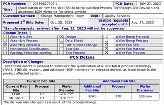
Part Number: LM2904 Other Parts Discussed in Thread: LM358B
Tool/software:
The internal structure of the chip of LM2904DR model does not match the standard sample. Is there a change explanation for the wafer modification? If possible, please help provide it. Thank you.
Is there a change explanation for the wafer modification?
This was the PCN issued in this part recently. Due to FAB change, the Si-die process and design have changed to the new process. There are some differences in the op amp between the old and new process due to the fab change, but the functionality and performance should be very similar.
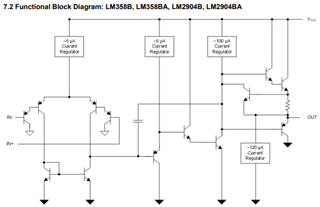
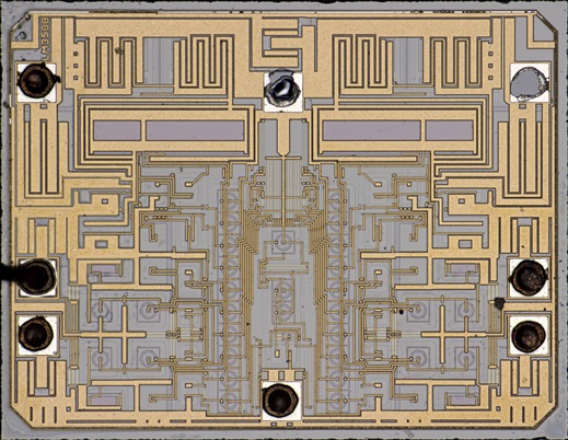
The image below is the internal structure and they should be nearly identical. Could you tell me what the internal structure of the op amp that does not match the standard sample?
The old fabs with wafers smaller than 300 mm were inefficient and were closed. The new die is the same as the LM2904B/LM358B and should look exactly like this: