This thread has been locked.

If you have a related question, please click the "Ask a related question" button in the top right corner. The newly created question will be automatically linked to this question.

LMH6703: LMH6703 output have 100mv sine oscillator noise

Part Number: LMH6703

Tool/software:

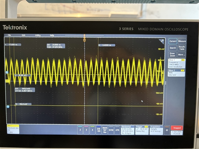
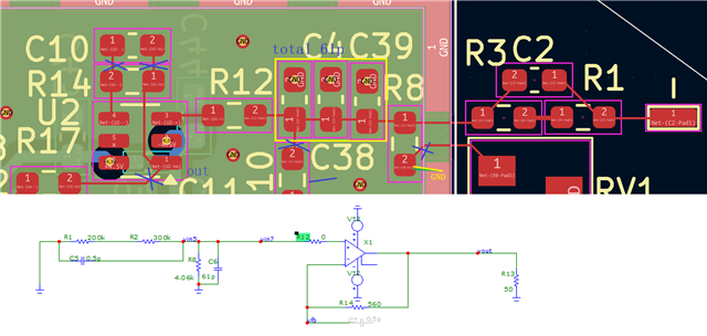
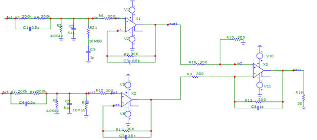
Here is my schmatic. The simulation result is OK , When I built a PCBA and the output have about 100mV sine oscillatoer noise?

Questions:

The above schmatic simulation is OK, when I designed a PCBA  and power(+/-4.5V) on . Here is my issues?:

1. if remove R2 ,R8,R20, floating In1,In2, why is Vin1=2V (about) Vin2=2V(about)?

2. add R2,R8,R20, floating In1,In2, why does output have about 100mv sine wave oscillation noise?

  • Hi Gary,

    Could you confirm if all the devices being used are LMH6703? If so one concern is the feedback configuration being used. For current feedback devices, we do not recommend any feedback capacitance as this can cause stability issues. We also recommend a minimum feedback resistance value, as this feedback resistance value ultimately affects the performance and the stability of the circuit. I would recommend changing the feedback resistance to 560ohms if in a SOT23 or 390ohms if in a SOIC. This is a good first step in trying to get the amplifier stable. 

    Best Regards,

    Ignacio

  • Hi Igncacio,

    Thanks for your help. Yes, I used LMH6703. Following your advice. I changed my layout to meet the below schamtic. I also testing the waveform. These are still have 764MHz oscillastion. Would you pls help me again? I used knife to cut C10, U2 Pin1 and solder a 100ohm resistor with Pin1 and ground. R8 Pin2 with gnd,Cut R10 Pin2. 

  • This is a 4 layer FR4 PCB and Signal/GND/GND/Signal layout

  • Hi Gary,

    Thank you for trying the suggestion I mentioned. One final option for us to try is simply removing everything and placing the circuit in a configuration we know should not cause an issue. If possible, could we remove all the components at the non-inverting input (R1, R2, C5, and C6) and placing 0-ohm resistors on R8 and R12. This would set the input directly to mid-supply without any additional components on that pin. The Rf resistor and R13 at the output to ground should be fine as long as nothing else is connected to the output node. After seeing the PCB layout, I was wondering if there were plane cutouts and around the sensitive nodes of the circuit (Inverting and output pin). With such a high-speed device, PCB layout is critical and could be the difference between a functioning circuit and one that oscillates. We do have layout guidelines in the datasheet that highlight best practices when designing with our high-speed devices. 

    Best Regards,

    Ignacio