This thread has been locked.

If you have a related question, please click the "Ask a related question" button in the top right corner. The newly created question will be automatically linked to this question.

TLV4062: TLV4062 the adjacent electrode for pin conductor.

Part Number: TLV4062

Tool/software:

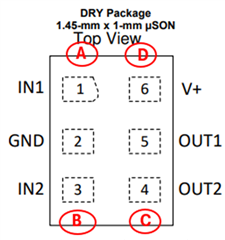
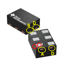
Target device: TLV4062DRYR 

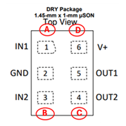
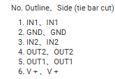
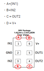
In the component outline drawing, a conductor (tie bar cut) is visible on the side of the component, but is this at the same potential as the adjacent electrode?

  • Hello Diasuke,

    The cuts adjacent to the pin along the long edge are connected to that pin.

    Looking at the drawings, I do not believe that there are the 2 cuts on the ends. I do not see where they would come from.

    There are many variations of this package. Most likely the datasheet drawing is generic and shows it as a precaution. My thought is that if they do exist, they are also tied to the end pin.

  • Question 1: Are the bottom electrodes and tie bar cuts (red) of No. 1 to No. 6 at the same potential?

    Pin Table

    No. Outline、Side (tie bar cut)

    1. IN1、IN1
    2. GND、GND
    3. IN2、IN2
    4. OUT2、OUT2
    5. OUT1、OUT1
    6. V+、V

    Question 2: Could you please tell me the electric potential of the diver cuts (A, B, C, D) on the side? Is it electric potential?

    Other side

    A=(IN1)

    B=

    C

    D

    Could you answer it?  Customer need to clarify this spec.

    Thanks and best regards,

    Daisuke Nomura

  • Hello Daisuke,

    If the cuts are present, I would assume they are connected to the adjacent pin.

    A=(IN1)

    B=(IN2)

    C=(OUT2)

    D=(V+)

    The leadframme drawing I see for the TLV4062 does not have these end cuts present. Just the ones on the sides next to the pads.

    The package drawing is generic to several different leadframe styles.

  • These are "pullback" pads; they are always at the same potential.


    (source: AN-1187 Leadless Leadframe Package)

    QFN packages can have extra tie bars to hold the lead frame during manufacturing:


    (source: Quad Flatpack No-Lead Logic Packages)

    I do not know how this works for SON packages; I guess the GND pad is directly connected to it.

  • I Looked at the drawing and bonding diagram pictures again.

    *IF* there is exposed cuts on the ends, it will be connected to that adjacent pin.

    This is a chip-on-lead package and there is no die attach paddle.

  • Paul-san, Clemens-san,

    Thank you for your answer.  Let me confirm as follows;

    - Regarding above Question 1,  I understand that they are the same potential. If not, please comment.

    TLV4062DRYR is made using the pullback method, so the bottom electrode PAD and the adjacent tie bar cut are at the same potential.

    Is it okay to assume that there will be no short circuit even if the PAD and the adjacent tie bar cut are connected with solder, etc.?

    Could you answer them?

    Thanks and best regards,

    Daisuke Nomura

  • With pullback pads, your PCB's solder pad should be entirely under the package (as shown in figure 18 above, and in the datasheet's example board layout), so there should be no solder at the side. But if there is solder at the cut, then it will not hurt.

  • Clemens-san,

    Thank you for your explanation

    Again, for question 1, Is it correct to understand that they are the same potential? let me confirm.

    I understand that the bottom electrode of the TLV4062 and the adjacent tie bar cut are at the same potential. Please let me know if there are any discrepancies.

    Thanks and best regards,

    Daisuke Nomura

  • Daisuke-san,

    What is your main concern? It seems we are talking in circles. Is this a PCB fabrication issue? Failure analysis?

    *Why* do you need to know the potential of the end cut-offs? You should not be soldering to them anyways...

    We have had NO problems with other customers since the introduction of this device.

  • Daisuke-san,

    I contacted the Engineer responsible for the DRY package.

    He confirmed the end cuts will be at the potential of the adjacent pins.

     ・A=(IN1)

     ・B=IN2

     ・C=OUT2

     ・D=V+

    I will close out this thread as I don't know what more we can say. If needed, we can get in contact internally.

  • Paul-san

    This is simple question.  Customer is considering assembly method and condition They will adjust the mask opening and adjust the amount of solder applied, but they asked if solder might adhere to adjacent tie bar cuts and cause a short circuit. Since the assembly side cannot check the electrical characteristics, they asked the manufacturing department (engineers) who have knowledge of the internal connections and structure of the TLV4062, "Are the bottom electrode and the adjacent tie bar cut at the same potential?"    I just want to confirm this answer. Could you answer it?

  • Hi Nomura-san,

    "Are the bottom electrode and the adjacent tie bar cut at the same potential?"    I just want to confirm this answer. Could you answer it?

    As Paul said, the non-side exposed metal (if present) will be the same potential as their nearest pins exactly as shown here:

    I've gone ahead and confirmed internally that the side exposed metal will be the same potential as their nearest pins:

    This is what you expected in your pin table: