Part Number: OPA354
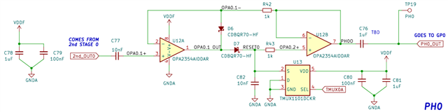
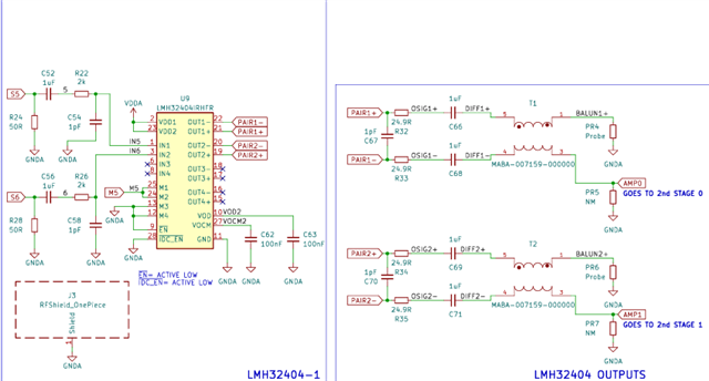
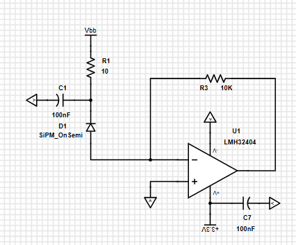
Other Parts Discussed in Thread: TMUX1101, OPA2354, LMH32404, LM7705, TINA-TI, OPA857
Tool/software:
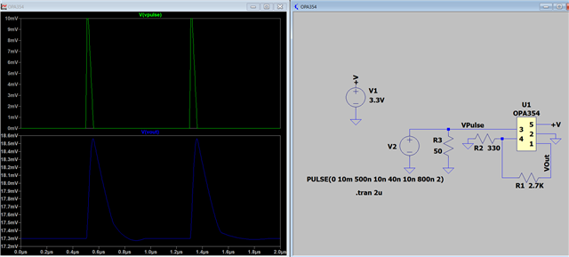
Hi,
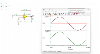
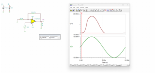
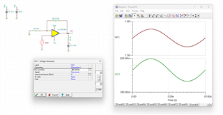
I still waiting some help about the problem with OPA354 using single rail power suplly simulation in LTSpice but I suppose it will be the some using PSpice TI_Orcad or I am wrong.
Best regards.
Andrea Papi