This thread has been locked.

If you have a related question, please click the "Ask a related question" button in the top right corner. The newly created question will be automatically linked to this question.

TLV7021: Purpose of via in detail

Part Number: TLV7021


Tool/software:

Hi team,

Could you explain that what the via in center pad can improve?

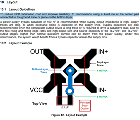
"To reduce PCB fabrication cost and improve reliability, TI recommends using a 4-mil via at the center pad connected to the ground trace or plane on the bottom layer."

If customer doesn't use this, what's expected to happen?

Best regards,

Hayashi

  • The datasheet recommends to route the ground (VEE) signal through the bottom layer. The alternative would be to route the signal between two other pads, which have a gap of only 0.326 mm (about 12 mil). Fabricating a trace reliably with such a small width and trace-to-pad cleareances would not be cheap.

  • Hello Hayashi,

    This device has fairly high speed edges (5ns rise/fall). So short traces are recommended.

    A narrow trace on the top layer to a solid ground probably will not cause too much trouble.

    As Clemens said, the clearances required really requires advanced PCB fabrication and assembly techniques.

    I would just recommend, as mentioned in the datasheet, to via-down to a lower plane and not try to run a trace between the pads. Place the bypass cap next to the VCC pin and via-down the cap ground to the same ground plane. Pretty much what is shown...