Tool/software:
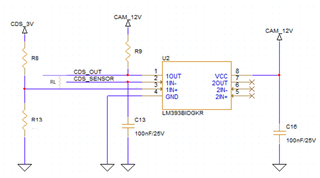
an you help me find the values for R8, R18, R9, and RL?
I want to set the initial voltage at the CDS_3V node, which is connected to the non-inverting input (+) of the comparator, to 0.48V.
The output of the comparator (CDS_OUT) should be between 10V and 12V when it is active.
When the comparator is triggered, I want to use a feedback resistor (RL) connected from CDS_OUT back to the non-inverting input (+) to increase the voltage at CDS_3V to above 2V.
Is there a way to achieve this behavior?