This thread has been locked.

If you have a related question, please click the "Ask a related question" button in the top right corner. The newly created question will be automatically linked to this question.

LMH6702QML-SP: LMH6702QML-SP

Part Number: LMH6702QML-SP
Other Parts Discussed in Thread: THS4304-SP

Tool/software:

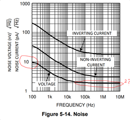
I need to make a noise analysis for my application using the LMH6702QML-SP. I know that the total noise will the sum of the:

  • Voltage noise: The amplifier’s input voltage noise has a gain to the output that traces out the noise gain curve shown earlier in the Bode analysis. Only the zero is considered here since we will assume a frequency of integration that is less than the pole and set by a post-filter. 
  • Current noise: The amplifier’s inverting input current noise shows up at the output times the feedback resistor. 
  • and Resistor noise: The resistor voltage noise shows up directly at the output with no gain. 

From the datasheet I got:

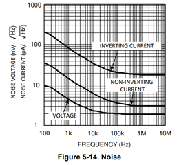
How can I compute that noise analysis? Do you have an excel table or noise tool for TIA?

Best regards, 

Franck

  • Is the graph of the Voltage noise normalized? I took the Low noise 1.83nV/√Hz given by the datasheet. Can you provide me the pA/√Hz for the current? I'm not able to find it in the datasheet. Thanks

  • Hello Franck,

       Quick question before the noise topic: do you need to use specific device? We usually do not recommend CFB amplifiers for TIA applications. The reason is because CFB are a bit tricky in terms of stabilizing especially when using input/feedback capacitance. It is possible, but would recommend switching over to a VFB amplifier. If you need space qualification, I would recommend THS4304-SP. Otherwise, if your project deadline is later in the next year. I will send over my email over private e2e messaging, we can discuss other options. 

      For noise, yes that is correct it would be a combination of those two specifications + your the noise from the photodiode. I would recommend looking over these collateral suggested below:

    1. TI Precision Lab Video Series, scroll down on right side, and please watch Noise (9), the first 4 videos are the most important
    2. E2E Thread where it walks through calculating output noise from TIA + comparing it to simulation
    3. Quick blog on TIA noise fundamentals

      Also below I attached two pdfs which I found very helpful on this topic as well. Please let me know if you run into questions/clarifications with suggested material.

    1727.noise11-Photodiode-Noise 1.pdf

    2870.noise12-Photodiode-Noise 2.pdf

    Thank you,
    Sima

  • Hi Sima, concerning the CFB device I used come from the fact that i need a TIA for space and with a slew rate > 2000V/us. From the Photodiode Design Tool:

    The values for RF and CF obtained from that TI tools  (CF = 4.57pF, RF =75 Ω) are conform to our calculations (CF = 4.7pF, RF =75 Ω) and allows:

    • a transimpedance BW: 507 MHz > 450 MHz
    • a low output noise : 174.1 µV rms
    • an input referred noise; 2.3 µA rms

    The basic requirements for the selected OPAMP for my application fit well:

    Parameter
    Value
    Supply Voltage ≤ ±15 V
    Output Voltage Range 0 - 3 V
    Analog Bandwidth (BW) 450 MHz
    fGBW > 1.57 GHz
    Low Noise NEP total design < 5 pW/sqrt(Hz)
    TID > 100 krad(Si)
    Operational Temperature Range -10°C to +75°C

    The THS4304-SP even qualified for space has a lower slew rate: 800V/us.

    Thanks, KInd regards

    Franck

  • Hi Sima, can you confirm that the graph of the Voltage noise is normalized? 

    Why 2 for the flat part?

  • Hello Franck,

      Thank you for the information and using our calculator. That is correct, with those selected values you would need a pretty high slew rate device. If you are okay with the design challenges in tuning a current-feedback amplifier as a TIA, you could use this device for your design. However, another option would be if possible to use two stages with first stage being the TIA using a VFB architecture which if you decrease the gain, you would not need to push an amplifier to needing a high slew rate, and the second stage can handle the rest of the gain. However, since noise seems to be critical for your application, this would increase your overall noise, but would need to check if it is higher than what you specified of 174.1 µV rms.

      The voltage noise is normalized, our amplifiers specify voltage noise as input referred (therefore not gained up, and we back calculate this + calibrate the other components in our usual test configuration out to obtain a true input-referred noise). We almost always title it input-referred voltage noise, but it seems like it wasn't specified in this specific datasheet. 

    Thank you,
    Sima