A related question is a question created from another question. When the related question is created, it will be automatically linked to the original question.
If you have a related question, please click the "Ask a related question" button in the top right corner. The newly created question will be automatically linked to this question.
The THS3491 can be set up in a difference amplifier configuration which would be the D2S portion of the circuit. For the buffered input stage, you could also use a THS3491 in a gain of 1V/V, however there could be other options as most current feedback amplifiers in a gain of 1V/V require some tuning as they tend to perform better at higher gains. In general, I believe every stage in the THS3217 could be replicated discretely using the THS3491. With implementing this circuit, the main consideration is ensuring the feedback resistance is in its optimal range for the gain being used and the package as this varies. Table 9-2 recommends the feedback resistors that should be used for a few gain configurations.
I would like to add that the THS3491 model was designed to only work in a gain of 5V/V. For the most accurate representation of the performance of this device, the datasheet would be your best reference. However, as I mentioned, I do not see a reason why this device could not function as a discrete version of the THS3217. I would also like to add that if considering this device or any current feedback device as a buffer, there is a feedback resistor that is required to keep the device stable. For the THS3491, we recommend around 2100ohms in a gain of 1V/V.
Thank you for the look up. I use two of BUF802 for my differential scope front input, and use the THS3217 D2S for my output. The THS3491 has higher LSB and sample setup than THS3217. now I can't judge which part is better for my design. any suggestion?
The THS3491 can be used as a difference amplifier and should not be a problem. You could use the BUF802 to buffer the signal and drive/amplify the signal using the THS3491 in a difference amplifier. Are there performance requirements you can share for your design? If you are looking for an amplifier with a wide large signal bandwidth, the THS3491 would be one of the better choices. Depending on what is required there might be another device I can suggest.
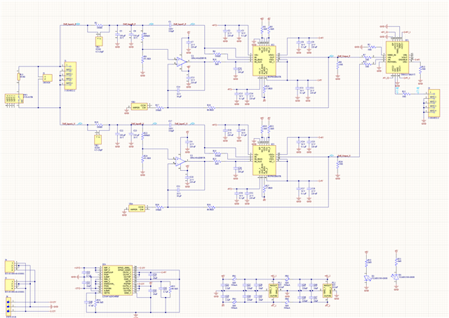
This is my schematic with THS3217, and it design for oscilloscope front input. it works up around 230MHz, and I would like to push the frequency as high as possible, and I have been thinking that THS3217 lower down the performance. The power supply circuit for THS3217 is complicate, and any recommend D2S amplifier that will support DC to around 1GHz in flat zone?
Is there a specific peak to peak you require for this bandwidth? It is a very wide bandwidth requirement especially when only considering the flat region and might be the difficult part of finding a device that would work. Also looking over the BUF802 circuitry, I am curious if you are seeing the expected results at the output of the devices. The input structure with the added 10Mohm resistor and capacitors (ex. C5 and C6) should change the response at different frequencies so I am curious if you are getting a flat response across frequency.
We did build and tested the design, the bandwidth is around 230MHz at 3db drop. The R1, R4 and R9 is 10:1 voltage divider, the C5 and C6 is the to increase the input capacitance, and that allow me to composite with VR1 capacitor. I will only install C5 capacitor and leave C6 open for 10:1 divider. I also notice that VR3 is no help much, should I remove it? and I need to design it onto 3X1.2 inch PCB which I try to limit amount on parts that I use.
Is the 230MHz being captured at the output of the BUF802 circuity? Are you seeing a clean signal with your testing. I am wondering if impedance matching is causing bandwidth issues. We had to tune the input stage to ensure a 50-ohm input impedance was maintained across frequency. As far as VR3, assuming it is also a potentiometer, we included it to tune the cross over region where the high impedance path would take over from the precision path to try to get as flat of a response as possible from DC to the high frequencies the BUF802 would operate at.
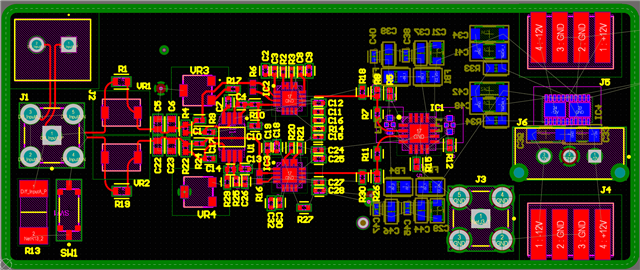
Thank you for reply. The BUF802 will work flat around 1GHz according with datasheet, and I can't find D2S OP-amp will work from DC to HF besides THS3217 and THS3491. I did connect the network analyzer to the circuit, it does show good flat BW around 230MHz, it is for entire circuit, not just output of the BUF802. The board was designed with 0603 package, and it has large spacing between the components. I agree that match impedance path with titer layout can improve the BW. This is my first high speed PCB layout, and I am working on Ver.2 layout. I use 0402 package this time, could you share some recommendation from your experience for my layout?
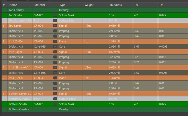
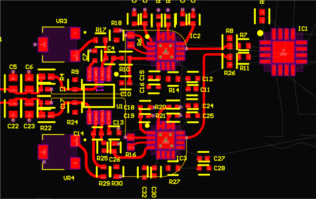
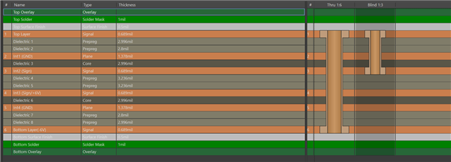
It is 6 layer board with FR408 with size of 2.9 X 1.2 inch. The board stack and layout at below
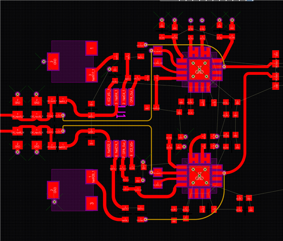
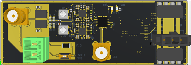
Can you share the Vpp you are setting to get the frequency response data. If it's a small signal, and the limitation is not in the BUF802 circuitry, the THS3217 should ideally have better bandwidth performance than 230MHz. If possible, could you try a small signal test if you have not done so already. For the BUF802 we got 1GHz by tuning the input circuitry to impedance match across frequency. I am curious if this could be a reason for the reduced bandwidth performance. I was able to look over the layout. One question I have is for your input, on your second branch (going through R19), that input is the SMA (J1) body from what I can see. Is this the intention of the circuit? I am wondering if this is also causing reflections of some kind resulting it lower bandwidth. I would suggest adjusting the decoupling capacitors from 0.1pF to 0.1uF, I am not sure this small of a capacitor would be all that helpful. I would also suggest putting the decoupling capacitors as close to the supply pins as you can. The row with C11 should ideally be moved closer to the pins. Overall, the layout does look compact which is ideal for something at these speeds. I would suggest looking over the layout we have for the BUF802EVM as this would be the best reference we have for how to ideally layout this device.
Thank you for the information and suggestion. I had tested this circuit with network analyzer which will be small signal test right? The VR1 and VR2 that pair with 10M resistor are adjustable capacitor. I add C5 and C22 to increase input capacitance of BUF802, so I have enough room to composite the capacitance with VR1 and VR2.(the C6 and C23 will be DNI, it is for future update for 50:1 or 100:1 divider) I agree that J1 SMA pair with J2 Molex will cause reflections, and the Molex is for twisted pair cable. Do you have suggestion or connector can improve the impendence issues? I changed the Input and output signal trace of BUF802 from top layer to layer 3 with blind via, the trace width can only be 3.7 mils according to Altium impendence calculation. should I stay on top layer? The Via size is 7mil hole with 11mil diameter and 4mil expansion top.
Yes, that is correct, if you were using some kind of network analyzer with a small signal (~100mV), your limitation in the performance should not be the THS3217 as it has significantly more bandwidth performance than 230MHz. This lower performance is likely due to the input structure of the BUF802 circuit. I assume you are trying to capture a differential voltage at two nodes; I am not sure what would be the best way to do this other than some kind of coaxial setup with an SMA like you have. For this circuit to work with a high input impedance setup, the tuning of VR1 with the capacitive network C5 (plus any parasitics) I believe would have to be precise in order to get the right response. Do you notice the bandwidth significantly changing as you tune VR1/VR2, whether it improves or degrades further? This would help us understand if the bandwidth performance is due to this portion of the circuit. For the layout, we try to limit any traces that via to different layers as this is not ideal for high-speed signals. However, we did via the feedback portion of the traces to the OPA140 but kept the feedback network close to the output of the BUF802. For the signals going into the BUF802, I would suggest keeping these on the top layer and try to get them as close to the input as possible, as additional trace length also results in inductance. I attached the BUF802EVM for reference on how we laid out this board.
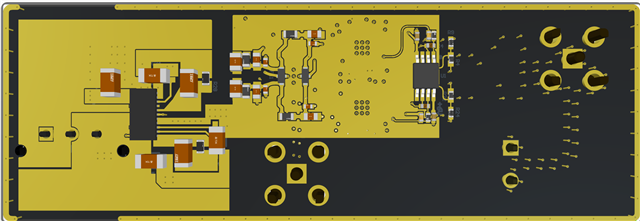
Sorry for the late reply, I re-layout and size down my board to 1 X 3 inchs. I followed with your recommendation above, and make all the HF trace on the top layer. The VR1 and VR2 will effect the frequency response if not tune it right. We have to calibrate each of them by hand. If this layout/design goes well, I will like try digital capacitor with edge card design. I want to calibrate it automatic with software. At last, could you take a look the THS3217 on my schematic? is there anything that I miss? Thank you.
I was able to look through your THS3217 schematic and I do have a couple suggestions. I believe for the VMID_in pin you can leave this floating if not using the buffer. R5 can be removed and would help reduce any space needed for the circuit. The same idea would apply to resistor R12 since you would not be using this path. For the input pins is there a reason you require the 50ohm resistors to ground? (R8 and R26) We have these on our board to impedance match with the previous stage's 50ohm series resistors. If everything is close together on a single PCB you wouldn't need to impedance match, and in this case the buffer is driving a heavier load by having those resistors to ground. R7 and R11 should be fine. For the pathsel pin, I would consider setting this pin high, which could cause the output of the D2S stage to go to pin 9 and leave pin 9 floating. I am not sure how the non-inverting input of the disabled OPS would behave so to be safe it might be better to set this D2S output to pin 9 as it is floating anyway.
Thank you for the review, and yes that path select pin should be high. I did experience some signal output at VOUT pin11 with disable OPS, and I was wondering why? Thank you again.
Ideally you should not see anything as it is disabled but potentially some signal is feeding through an input diode and is being seen at the output through the feedback resistor but ideally it should not be seen.