This thread has been locked.

If you have a related question, please click the "Ask a related question" button in the top right corner. The newly created question will be automatically linked to this question.

OPA690: Help with Hardware Comparator Design for Hall Sensor Signal without Negative Supply.

Part Number: OPA690
Other Parts Discussed in Thread: TINA-TI, TLV3541, OPA357, OPA354

Tool/software:

Hi,

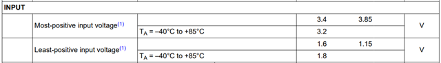
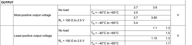
I’m currently designing a hardware comparator circuit that generates a fault signal to the MCU based on current thresholds. The input to this comparator comes from a Hall-effect current sensor, which outputs an analog signal that swings both positive and negative (approximately ±1.4 V peak).

Design Constraints:

  • The system does not have a negative power supply rail available.

  • I need to detect both positive and negative peak thresholds.

  • The comparator and signal conditioning must operate from a single positive supply (e.g., 0–3.3 V).

  • The comparator input range should be within ~0.1 V to 2.9 V (to allow margin inside a 3.3 V rail).

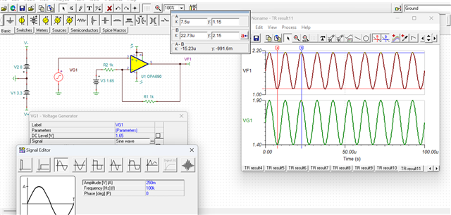
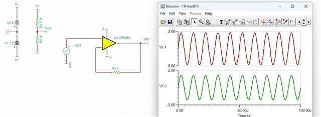
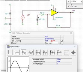
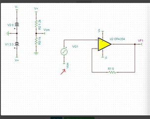
To address the lack of a negative rail, I used the OPA690 to add a DC offset, level-shifting the input signal such that the original ±1.4 V signal is shifted to ~0.1 V to 2.9 V.

  • This method worked fine in LTspice with generic components.

  • However, when I simulated the actual circuit in TINA-TI using the OPA690 model:

    • Without the negative supply connected to the OPA690, the output became erratic.

    • When I added the negative supply, the circuit performed as expected.

Solution Required:

  • Could you please suggest a better solution to design a hardware comparator for this requirement without needing a negative supply?

  • If the DC level-shifting approach with the OPA690 is viable, please help me understand:

    • Why does the circuit behave incorrectly without the negative rail?

    • Is there a way to modify the design so it works reliably on single-supply operation?

    • One more issue i faced was the comparator outputs was not straight, and not constantly same. Is this issue because of op-amp input for the comparator?

I have attached the simulation waveforms for both cases (with and without negative supply). Kindly let me know if I’ve made any mistakes or missed any considerations.

Thank you for your time and guidance.

  • Hi, is there any update over this. Can you please provide solution on this.

  • Hello Karthick,

     I apologize for the delay in response for your issue, and thank you for laying out all the details and for using Tina-TI, it made it very easy to follow and pinpoint the issue.

     You are correct for system block diagram layout: using an amplifier to offset voltage for single-supply type applications. And, it is good you are accounting for headroom. The issue is the chosen amplifier OPA690 will not be able to output 0.1 V to 2.9 V. For that range, you would need a rail-to-rail output amplifier to avoid violating the output common-mode range of the device. Also since your input will be +/-1.4V, the amplifier will not be able to accept a negative value at the input since it will violate the input common-mode range of the device. In application statement, it was mentioned your input is a current sensor, would you though need to convert this to a voltage prior to the input, in that case you would need to use a TIA (transimpedance) type of amplifier configuration. But, I think hall sensors are usually voltage outputs, so will continue with below recommendations. 

    Example with OPA690:

      For example to demonstrate the issue using the OPA690:

      Below is the input and output voltage range of the device:

      These specifications are for single 5V supply configuration. When you convert to 3.3V supply, then your input voltage range is 1.15 to 2.15V, and your output voltage range is around the same as well. 

       Taking this into account, below is a working example of the full-range of the OPA690, you would need to level shift the input to mid-supply (or any other voltage that would work within the range, mid-supply is most recommended for full-range). Then, I selected an example of +/-250mV input, which will give a +/-500mV output level shifted at 1.65V. 

      Therefore, for +/-1.4V, I would have a gain of 1V/V instead, then select an amplifier that can handle that input and output level shifted. Also note: after doing the simulation, I realized the device min is 5V and not 3.3V, but simulation will still work since our models do not have a min/max voltage error, but will do headroom ranges and clamp accordingly. We will take this into account for device chosen in the next example. 

    Example linked to your design requirements:

      I would instead suggest to use any of these amplifiers: filtered link. If your input will be 2.8V centered around a voltage: for example let's say 1.5V: then your input voltage will be from 0.1V to 2.9V as design requires. This would mean from the filtered list linked in the previous sentence, you would need to choose the devices that are rail to rail in and out such as the TLV3541, OPA357, OPA354, etc. If you are able to attenuate your signal prior to input of amplifier via a simple voltage resistive divider network, or increase your rail supply to 5V single, then you can choose the devices that are Out or In to V-, Out. 

      I will use the first suggestion to fit initial requirement and select OPA354, but you can change it if you think the other suggestion will lead to a better choice in amplifier in terms of bandwidth or any other specifications.

      In this way, it will be a simple buffer, and you can level shift the input at the amplifier as a voltage divider from the rail as shown in the sim above (In the previous example I just added it as a DC offset in the source, but would need to apply this on the board after your sensor).

      Also, here is a quick app note on single-supply applications to explain above in equations instead of simulations: https://www.ti.com/lit/an/sloa030a/sloa030a.pdf? 

    Thank you,
    Sima

  • Thank you for your previous response and the proposed solutions. I appreciate the support, but I would like to clarify my specific requirements and constraints to ensure the correct approach.

    My input signal is a sinusoidal waveform swinging from +1.4 V to -1.4 V, originating from a Hall effect current sensor. However, my circuit operates on a single positive supply only (e.g., +3.3 V or +5 V), with no negative rail available. Therefore, I need to level-shift the bipolar signal to a unipolar range suitable for further signal processing using an op-amp-based circuit.

    Concerns with the Provided Solutions:

    • Solution 1: It appears the sine wave generator is already producing a level-shifted signal with a 1.65 V DC offset. However, in my scenario, I do not have control over the sensor output, and this level shifting must be done using an analog circuit, not at the source.

    • Solution 2: This approach connects the signal source to a voltage divider biasing network (Vcm). However, since the Hall sensor output is referenced to ground, I cannot float it or reference it to a midpoint voltage(Vcm). Any level shifting must be done post-sensor, keeping its ground-referenced nature intact.

    Requirement:

    I need an op-amp-based level shifting circuit that:

    • Accepts a ground-referenced ±1.4 V signal,

    • Shifts it to swing within a unipolar range (e.g., 0 V to 3 V),

    • Operates from a single positive supply only.

    Additionally, I need to design a comparator stage that detects when the original signal crosses ±1 V thresholds. Since the signal is level-shifted to the positive domain, the comparator design must appropriately set threshold levels corresponding to the shifted equivalents of +1 V and -1 V from the original signal.

    Thanks in advance.