This thread has been locked.

If you have a related question, please click the "Ask a related question" button in the top right corner. The newly created question will be automatically linked to this question.

INA333: INA333

Part Number: INA333
Other Parts Discussed in Thread: INA826

Tool/software:

Hello TI Team,

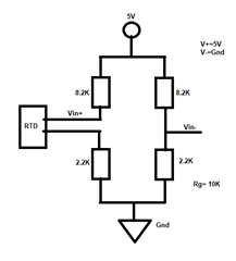
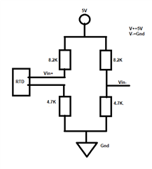
I intend to interface the 3 wire RTD with the INA333. Could you please suggest the design for it ? 

I appreciate your feedback. Please revert asap.

-----------

Regards

Jigar Jain

  • Hi Jigar, 

    We have design guidelines to help guide through the design with a different device, INA826, but similar design steps can be applied to the INA333: Link

    Do you have specific questions related to the design? 

    Regards,
    Ashley

  • Hello Ashley,

    Thanks for the update. As per the datasheet, the Vcm range is V-(+0.1) to V+ (-0.1V). But above 0.2V to 0.8V range, the op-amp is not workable. Could you please let me know why it is not working? See the below image for reference. Could you please look at it and let me know what the issue is with this?

    Regards

    Jigar

  • Hello Ashely,

    I have tested the design with below configuration with the change of the gain resistor but do not get the proper output.

    Please look at it and let me know the issue. 


    Vin+ Vin- Diff Gain Vout as per Gain Actual
    0.94 0.899 0.041 11 (10K) 0.451 0.447
    0.928 0.899 0.029 11 0.319 0.321
    0.915 0.899 0.016 11 0.176 0.188
    Vin+ Vin- Diff Gain (2K) Vout as per Gain Actual
    0.94 0.899 0.041 51 2.091 1.845
    0.928 0.899 0.029 51 1.479 1.477
    0.915 0.899 0.016 51 0.816 0.862
    Vin+ Vin- Diff Gain (1.67K) Vout as per Gain Actual
    0.94 0.899 0.041 60.88 2.49608 1.853
    0.928 0.899 0.029 60.88 1.76552 1.749
    0.915 0.899 0.016 60.88 0.97408 1.018

    Could you provide the TINA model to simulate this application? 

    Regards

    Jigar Jain 

  • Hi Jigar, 

    Could you clarify how you are configuring the INA? What is reference pin connected to and do you have any loads connected to the output? 

    Regards,
    Ashley

  • Hi Ashley,

    Please see the reference image that I have provided, where the Vin+ and Vin- connections that are connected respect to PIN3 & PIN2 of the Op-Amp. About reference pin 5, It is GND. There is no load connected at output Pin 6. The supply voltage of the op-amp is 5V, and the Wheatstone bridge voltage is 2.5V. (In image mentioned 5V, which is wrong mentioned). 

  • Hi Jigar, 

    Thank you for the information. With the conditions mentioned above, you are limiting the output voltage swing range which is why the actual output is not as expected. This behavior cannot be seen in simulation and is calculated via the Vcm vs Vout plots or using the Analog Engineer's Calculator

    I recommend trying to change the resistor values to increase the input-common mode voltage or increasing the wheatstone bridge voltage to see if this helps to fix the output issue. 

    Regards,
    Ashley

  • Hello Ashely, 

    What do you mean? Do you mean increase the Wheatstone bridge voltage 0.9V to 1.2 or above?  Pracitcally does it work ?

    Regards

    Jigar Jain 

  • Hi Jigar, 

    The common mode voltage is determined by the resistor divider that is constant in the Wheatstone bridge (Vin- leg in this example). So, depending on the excitation voltage and resistor ratio, this will change the voltage measured at Vin- and change your input common mode. I've attached a TINA simulation showing different examples of how this voltage changes with the different excitation voltages and if you add a resistor between the bottom leg and ground (R5). The design information on this is further explained in this reference design: Single-Supply Strain Gauge in a Bridge Configuration Reference Design


    wheatstone-bridge-e2e-jigar.TSC

    Please let me know if you have further questions.
    Thank you!

    Regards,
    Ashley