This thread has been locked.

If you have a related question, please click the "Ask a related question" button in the top right corner. The newly created question will be automatically linked to this question.

INA333: Monolithic Instrumentation Amplifiers and Driven right Leg (Please Ignore the Part Number)

Part Number: INA333
Other Parts Discussed in Thread: TINA-TI, TLV9351

Tool/software:

Hi,

I'm trying to add right leg drive to my design, and have a couple of questions. I get the concept well, but most of the papers/docs/articles/videos I have seen online from multiple sources don't explain all of the components or how I would calculate appropriate values, so I have a few unknowns still.

Note: a lot of walkthroughs/derivations of DRL take the common-mode signal from the output of the two buffers, as this is enough to demonstrate things conceptually. I'm not looking to make my own INA from discrete opamps, so, all of the below applies to implementing DRL using the common-mode signal from the external gain resistor.

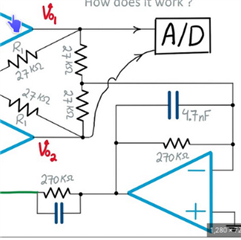
1) Gain resistor network.

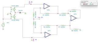
Some designs I see tap the common-mode signal across two gain resistors:

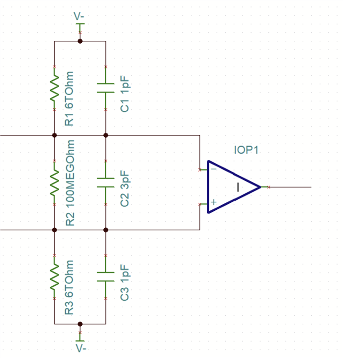
Other designs add a third in parallel with these two:

Could anyone please explain the reason for this third resistor? Is it just for component matching/tolerance, or does it relate to having a buffer or not before the inverting amplifier? How should I select appropriate values for the downstream amplifier and for the appropriate gain of the INA?
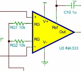
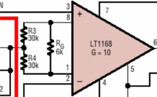
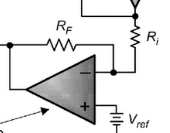
2) Use of Buffer

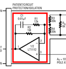
Some designs feed the tapped common-mode signal straight into an inverting amplifier:

Other designs have a buffer in front of the inverting amplifier:

What are the advantages of this? Is it to prevent any instability in the inverting amplifier from entering back into the common-mode signal in the INA?
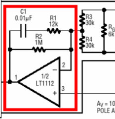
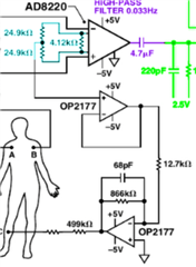
3) Filtering

Basic designs just use a resistor network for setting the gain of the inverting amplifier and a short-protection resistor:

Others include a lowpass filter and a stabilising filter:

I see others using a high-pass filter(?) too:

My basic understanding is that the filter is to reject high-frequency noise that's outwith the signal passband anyway. And also because most INAs have lower CMRR above ~10-20kHz, so we should just neglect that range. If I am filtering this on the amplifier inputs anyway, then I shouldn't be trying to feed that back in.

Should the corner frequency of the lowpass be roughly matched to my input filters? I.e., the -3dB of my RFI filter is about 45Hz, as I am working with EEG and anything above this is out of range for my application. Is the idea that I should filter out roughly the same frequency range on the inverter?

Then, I assume that the stabilising section is to prevent resonance in the feedback network - we need to dampen the signal as we're using negative feedback so an impulse in the common-mode signal at the inputs could cause the DRL circuit to oscillate violently back and forth. Is there a guide on how I could calculate appropriate values for this, or can I use a generic reference on attenuating negative feedback loops when using opamps? I've seen the concept of resonance in other contexts before, but not specifically in electronics, so, I think I could probably look up a general circuit template and work with that - but soe of it might go over my head a bit and I'm not sure if there are special considerations I need to take into account here.

Would anyone be able to help me or point in the right direction on these points please? Or know any resources on how to choose the specifics of implementing an RLD subcircuit? As I'm finding a lot of guides going over the concepts, but at my low level of electronics understanding, I'm struggling a bit to translate this into a specific schematic that I can use.

Thank a lot for your help!!

  • Hello again Ben!

    1. Gain networks.
      The variance in different gain resistor networks could either be to target a specific thevenin equivalent resistance, but the ultimate goal is to generate a voltage reference point that is equal to the common-mode of both of your input amplifiers. Handily, the midpoint of the voltage across Rg is your common-mode.
      Below is a circuit created with ideal components. The input VCVS devices are configured to allow VG1 to set the input voltage differential, and the DC source VCM to set the input voltage common mode. In an instrumentation amp, the value of the input common-mode voltage is going to be the average of IN+ and IN-, Vinp and Vinm. If you were able to tap the exact midpoint of a single gain setting resistor, the voltage at the middle of that resistor would be equal to your VCM. Since most resistors don't have a midpoint tap, we use two resistors and tap the midpoint there, and do the math to get the correct equivalent resistance. Ultimately the Instrumentation amp (IA) does not care if you have two series resistors, or 500 series resistors, it cares about the equivalent resistance seen between the RG pins, so to the function of the IA is unchanged, and you have a handy point where you can sense the common mode.

      Here's the TINA-TI sim if you would like to poke around: Ben_Ideal_INA.TSC
    2. To buffer or not to buffer?
      Similar to the above topic, the gain of the instrumentation amplifier will be governed by the impedance between the RG pins of the IA. If your feedback network is sufficiently high impedance to not disrupt the equivalent impedance seen at RG, the buffer is unnecessary. If you do not want to do the equivalent resistance math, buffering the signal adds all the non-idealities of the buffer amp to your common-mode signal at the trade off of almost no loading to your gain resistor network, due to the high impedance inputs of the op amp.
    3. Filtering
      This feedback system can introduce significant amount of phase lag in the total feedback loop. This can cause instability, there is a slide deck that is essentially a picture book that goes over some of the rate of closure analysis of the feedback loop, although it employs a surprise different architecture where the common-mode of the IA is driven by a separate amplifier.
      https://www.google.com/url?sa=t&source=web&rct=j&opi=89978449&url=/cfs-file/__key/communityserver-discussions-components-files/14/RLD.pdf&ved=2ahUKEwii85WE_vuNAxVPLtAFHTaHANsQFnoECBwQAQ&usg=AOvVaw0wzUJg0Am3MDFtY1Yaagf6

      Here is a paper describing a similar type of compensation that is applicable to DC/DC converters, but is similar in implementation.

      https://www.ti.com/lit/an/slva662/slva662.pdf

    Best,
    Gerasimos

  • Likewise! I had wondered if Ed/Edd/Eddy might be the first to reply :)

    Okay, thank you, I had not thought in these terms but I think I am understanding 1) and 2) - it's effectively just the series resistance that the OpAmp sees. So for high gain we want a low-value gain resistor, calculated according to the datasheet. If this goes directly into a high input-impedance opamp with low input voltage noise and low bias current, etc., then we should be golden. But if we are using an inexpensive or even real-world opamp, this may not be the case.

    So we are simply juggling:

    • the impedance of the resistor, seen by whichever OpAmp first in the feedback chain as its source impedance
    • the input impedance of that OpAmp
    • Thermal noise over the resistor muddying the common-mode signal sent to the feedback network
    • Noise pollution into the gain network from the feedback network.

    And as an addendum, we might have other components for various reasons in front of or in parallel with the input pins of the Opamp, as in the 12.7k in the screenshot above with the cyan/green/purple text. I'm not sure why it's there, but if it's needed for the feedback network., the buffer stops it becoming part of the resistor network too.

    All so that in a totally ideal world, zero current flows from the tap in the gain resistor network to the OpAmp, zero noise or stray voltage from the OpAmp affects the gain network, and the network sets the appropriate gain(?) We therefore use the third resistor in parallel with the other two if we can't find a good solution with just a 1:1 voltage divider.

    And for the buffer, if we are using a lowpass filter on the inverting amplifier like this one:


    the capacitor is offering high-frequency signals a way to bypass the high-impedance input of the OpAmp and thus loads the gain resistor at high frequencies. If there is a slight mismatch above in the two gain resistors, meaning one is 26k and one is 28k, we're creating a differential signal before the subtractor stage and degrading CMR quite badly. I assume even if they were perfectly matched, we might degrade the CMR of an ideal component three-OpAmp for some SparklesreasonsSparkles I can't put into words right now (I should have a play with your simulation and see what happens! I knocked up a similar one myself so would be good to compare them, thank you for that) or alternately for a real-world monolithic InAmp, given that the internals of how they work are more complicated than the ideal equivalent circuit. Either way,

    I have been thinking of buffers a bit like a way of "pinning" a voltage. Would it also be fair to say they could be conceived a bit like an AC current diode? Not in the sense of direction of conventional current or positive/negative voltage as with a real diode, but in the sense it forms a barrier between separate sections of the circuit preventing one stage from loading another. They have high input impedance, low output impedance (able to source and sink current), so, another way to think of it is if I rotated the triangle 180 degrees, that's pointing in the direction a (non-negligible) amount of current can flow. When driving the reference pin, current can flow in either direction between the INA and the OpAmp's output; in this setup, only a negligible amount of current can flow in either direction between the buffer and the gain resistors. So I should perhaps consider using one in situations where I want one stage of a design to be logically separated from another.


    On 3, I will read that in due course; the link is broken for me but looks like it should be this, for reference if anyone else is reading.

    /cfs-file/__key/communityserver-discussions-components-files/14/7838.RLD.pdf

    I did have a copy of those; hopefully would be easier to digest with the notes/audio accompanying it so I might see if I can find a video or anything going with the slide desk!

    Thanks again, and sorry for a bit of a wordy reply as I talked myself through things!

    Ben

  • Ben,

    But if we are using an inexpensive or even real-world opamp, this may not be the case.

    Yes, but you can verify with the input impedance spec of the op amp, and it need not be expensive. The TLV9351 has the following input impedance, and the equivalent resistance network can be seen below.

    For ease of math purposes, we can assume that the impedances are tied to V- of the amplifier.

    Generally the RG resistors should be high precision and low drift, as they govern the gain of the input stage and can dominate the error if they are imprecise.

    The addition of the 12.7k resistor is there to set a maximum gain of the error amplifier.

    Even in the ideal 3amp InAmp, upsetting the matching and ratios of the resistors encircling the perfect amplifiers will show the correct degradation of CMRR, as the resistor matching is the governing source of error in these cases. The op amp CMRR is usually >120dB, whereas the CMRR due to resistor matching is at best around 100dB. There are some devices that achieve better matching, but generally across the gamut of CMRR in difference amplifiers, which is what the third amp is doing, with today's resistor matching best practices, that's about where they fall.

    I'm not sure I fully followed your AC current diode comparison, but it is correct that generally buffers are employed to faithfully replicate the voltage on a sensed node without applying loading effects to that node. This is due to the ideal properties of amplifiers that you mentioned. The way that I think of op amps are simple feedback machines. The op amp can control only one node, the output, with the ultimate goal of driving the inverting feedback node IN- to be equal to IN+. Applying a resistor network in feedback provides a scaling factor that the output must obey to set the inputs equal, but ultimately that's the fundamental workings.

    Best,
    Gerasimos

  • Sorry for the long delay, had my hands full and not had time to look back at the DRL until now!

    So then, is the resistor network more just about picking a third resistor to cancel out any mismatch in the tolerances in the first two? I guess I'm a bit lost as to where I should start in choosing values and how to hook the inverter in, for a given equivalent resistance/gain and given OpAmp.

    Thanks again

  • Hey Ben,

    No worries! Yes, adding a sufficiently smaller third resistor will cause the smaller resistor to dominate the error analysis. If you are looking at how to add in an integrator, the easiest method would be to buffer the mid-voltage point. This will remove the need to calculate complicated resistance networks and their resultant effects on the equivalent Rg.

    If you have a matched pair of resistors that has good absolute and relative tolerance, this could be a good candidate, as you will not need to use two imprecise resistors and one precision parallel resistor.

    Best,
    Gerasimos