This thread has been locked.

If you have a related question, please click the "Ask a related question" button in the top right corner. The newly created question will be automatically linked to this question.

INA168: Power supply is unclear and need examples

Part Number: INA168
Other Parts Discussed in Thread: OPA333, INA138

Tool/software:

Hi,

my customer asked about the power supply of INA168 (and OPA333) in app note SBOA198A:

Questions

Could you please give me a clear example of what a correct/complete design must look like including the power supply?

In Lightning events, the voltage becomes negative (-100V at the load).

  • What current is measured?
  • Does the output remain "stable" and return when the voltage is >0V?
  • If my "switch" is closed (no connection to the battery), a CM voltage of -100V is set
    • That is correct?
    • If the device suitable for this or there is a workaround?


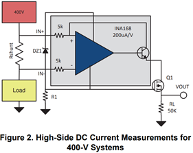
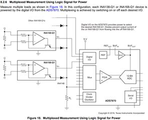
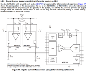
Can I use the circuit from the INA168 datasheet according to Chapter 8.2.6 if I do not supply V+ from a GPIO but want to build it floating like in Figure 2 from the app note.

Can I use the circuit from the INA168 data sheet according to Chapter 8.2.5 if I do not want to supply V+ with 5V but want to set up floating like in Figure 2 from the app note.

  • What is the negative CM voltage that sets in?

Best regards

  • Franziskus,

    This app brief alludes to this TIDA: https://www.ti.com/lit/ug/tidu833/tidu833.pdf?ts=1750784387877 which shows the schematic for this topology in full. Unfortunately, even in this configuration, if the load were to become -100V, this would likely cause an absolute maximum violation of the common mode voltage of the device. The design uses the Zener diode to create a virtual GND that is held to a strict voltage beneath the device (ie, a 10V diode in a 400V application as shown in the document would create a GND of 390V). This in effect creates a floating supply and is how the design can achieve the higher common mode voltages shown. However, the abs max voltages for the common mode are taken with respect to that same ground, which is based off the load voltage, so if the load were to become -100V, this would apply -100V to the inputs of the device, and would be a violation. 

  • Dear Carolus,

    thank you for your answer.
    The question was by me.

    Please can you answer my other questions to bipolar measurement and multiplexed measurement.

    If it is possible to supply the INA with the output signal, after the high side switch? 
    And how long is the response time between switch turned on and current measurment is correct?

  • Michael, 

    I don't quite understand what you are asking here: "If it is possible to supply the INA with the output signal, after the high side switch?" What output signal are you referring to here, and where in the circuit would you place the high side switch? 

    Regarding the bipolar and multiplex options, yes, I would expect you could place TIDU833 inside of the diagrams you show and this should work. Once you move below the pedestaling FET in the design you would be back at normal levels in terms of voltage and could handle the current based signal as you normally would with a resistor at the point of the ADC. However, I cannot answer the expected time to first steady state measurement. This would likely be a complex function of the device, FET, and ADC chosen for the application. I would recommend pulling down the INA138 or INA168 spice model as well as a SPICE model for the chosen FET and simulating it for expected behavior.