This thread has been locked.

If you have a related question, please click the "Ask a related question" button in the top right corner. The newly created question will be automatically linked to this question.

OPA301: TIA using OPA301-BW calculation

Part Number: OPA301
Other Parts Discussed in Thread: LMH32401, OPA857, OPA855

Tool/software:

Dear Team,

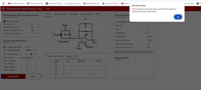
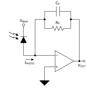
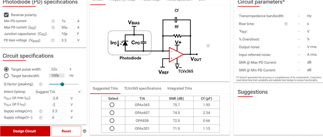
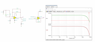
My circuit is given below.

I used this equation for calculating the bandwidth of the TIA.

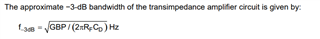
My RF is 200K and Cd is 1.3pF(diode) + 9pf (Opamp input capacitance).

After calculation I am getting a value of 11Mhz and simulated value is 800K.

May I know why such a difference.

OPA301.TSC

Regards

HARI

  • Hello Hari,

      I apologize we missed your thread.

     The equation used is the correct approximate for -3dB bandwidth. However, this equation is simplified for approximation since for accurate bandwidth calculations, we would need to use the full transfer function which would incorporate Q factor which is related to selected feedback capacitance. 

      In simulation, if you vary the feedback capacitance, C1, this will vary your closed-loop bandwidth. The one you have chosen is 1pF, which would give you a very stable circuit for the chosen values. If you lower the feedback capacitance to 0.3pF, this would adjust your Q factor to around 0.707 which is considered "Butterworth response" which means the AC response passband is maximally flat with no peaking. Our old TIA calculator is giving around 3.41MHz of bandwidth in this case. Increasing feedback capacitance will increase circuit stability (lower peaking), and therefore leads to lower closed-loop bandwidth.

       New TIA calculator: https://dev.ti.com/gallery/view/TIA/TIA_GFN/ver/1.0.4/

       Old TIA calculator:  [FAQ] Transimpedance Amplifier Calculator 

      If you are interested in the full TIA analysis equation rather than the approximate form given, here are some good app notes on the concept:

    1. https://www.ti.com/lit/an/sboa122/sboa122.pdf
    2. https://www.tij.co.jp/jp/lit/an/snoa942a/snoa942a.pdf
    3. https://www.ti.com/lit/an/sboa055a/sboa055a.pdf
    4. https://www.ti.com/lit/ab/sboa354/sboa354.pdf?
    5. https://www-f9.ijs.si/~margan/Articles/trans_z_amplifier.pdf

    Thank you,
    Sima 

  • Hi Sima,

    No issues.Thank you very much.Whenever I use TIA Calculator.I am getting this error shown below.

    May I know What mistake I am doing.I need positive reverse bias.The tool says polarity is wrong.

    Regards

    HARI

  • Hello Hari,

      Thank you for using the calculator.

      The reason why you are getting this error is because depending on your photodiode chosen, you would either need to apply a positive voltage bias or negative voltage bias to your photodiode for operation. Typically these diodes are designed to be reversed biased which means an external voltage needs to be applied which simply would be the cathode would have to be more positive than the anode. 

      An example using a diode with a negative voltage bias is from LMH32401 datasheet: (sinking current configuration: device is being used with a PD that is configured with its cathode tied to the amplifier input and the anode tied to a negative supply voltage). This means the current out of the diode is positive, and voltage at the output of the amplifier swings above the voltage reference set. The voltage reference at the amplifier pin (IN+) needs to be tied to a higher potential compared to the diode's reverse bias for proper diode operation. (Note: for LMH32401, it has a specific VOD pin and differential output amplifier integrated so it will be a bit different for this specific amplifier) 

      Second Image is from ThorLabs: shows simple VFB amplifier can be used with same connection PD with either grounded or negative voltage bias.

       An example using a diode with a positive voltage bias is from the OPA855 and OPA857 datasheet: (sourcing configuration: device is being used with a PD that is configured with its anode tied to the amplifier input and the cathode to a positive supply voltage). These connections make sure that the photodiode sources an output current that results in the amplifier voltage output swinging down below the reference voltage. The voltage reference at the amplifier pin (IN+) needs to be tied to a lower potential compared to the diode's reverse bias for proper diode operation. 

      In the TIA calculator, the reverse polarity shows second example. Therefore, Vbias should be positive voltage, and Vref should be lower value than Vbias for correct diode operation. (Technically it doesn't have to be positive, the second part is only critical for operation, so for example you could have -1V bias, then Vref at -2V, however this could depend on the diode chosen which will specify voltage bias vs internal PD capacitance). I couldn't find a way to chose your own Voltage reference value, this is probably the main confusion, I will let the designer know about this issue and will see if we can include having a way to choose this value. 

      Therefore, currently for it to work in the reverse polarity, you would have to change the output voltage to negative for the calculator to work:

      The calculator is incorrect in terms of the output voltage in reference to set amplifier supply voltage. I will also let the designer know about this, it probably was set like this to calculate pulse is negative in reference to Vref, rather than actual negative output. Like shown in OPA857:

    Thank you,

    Sima 

  • Hi Sima,

    Thank you.

    Regards

    HARI