This thread has been locked.

If you have a related question, please click the "Ask a related question" button in the top right corner. The newly created question will be automatically linked to this question.

OPA388: Regarding use of OPA388 for reference buffer.

Part Number: OPA388
Other Parts Discussed in Thread: OPA350, THS4281, OPA333, OPA328, TINA-TI

Tool/software:

Hello TI support,

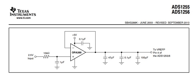
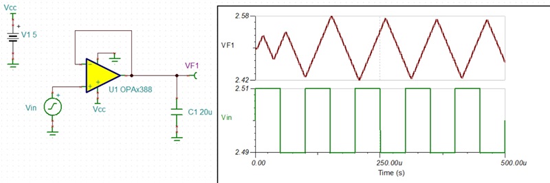
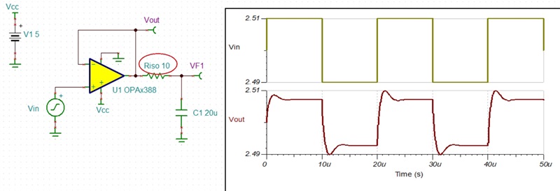
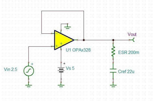
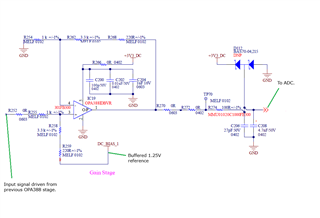
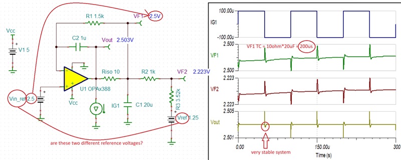
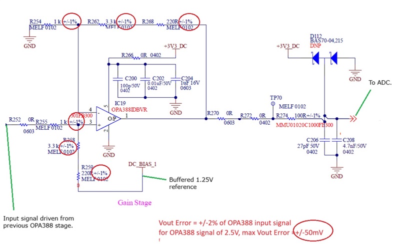
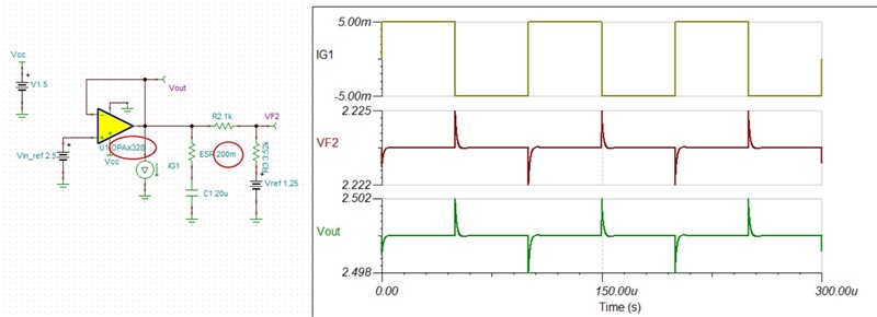
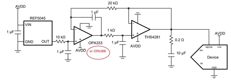
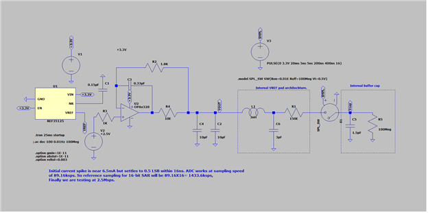
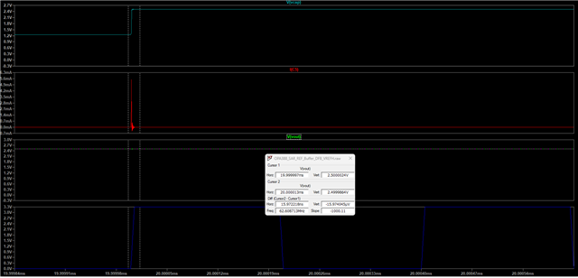
Can we use use OPA388 as reference buffer for 16-bit SAR ADC with 2X 10uF tantalum capacitor as its output load? If not, please suggest suitable precision opamp supporting 3.3V supply range.

Regards,

JK

  • JK,

    There are very few op amps that could directly drive (with no series output resistor) 20uF cap and the one that comes to mind is OPA350 - see example below.

    However, OPA350 is nowhere near the precision of OPA388 chopper amplifier but no zero-drift amplifier can directly drive 20uF loads.  Thus, in order to assist you, it would be very helpful to understand whether you are considering OPA388 zero-drift amplifier due to its very low Vos, temperature drift, or both?

    You could use OPA388 but in order to be stable it would require an isolation resistor, Riso, of 10 ohm or higher - see below.

    Also, if minimizing the total power consumption is critical, you could use a composite amplifier with OPA333 zero-drift assuring precision while THS4281 controlling the settling time - see below.

    In case the power is not important, the simplest solution may be to use OPA328 with 0.2ohm ESR - see below.

    https://www.ti.com/lit/an/sboa558/sboa558.pdf?ts=1751496183504&ref_url=https%253A%252F%252Fwww.google.com%252F

  • Hello Marek,

    Thanks for providing detailed response covering all aspects. Yes, actually we are already using OPA388 in our circuit and was thinking to use same because of its precision characteristics & BOM reasons. 

    I recall one appnote having different solutions for stability where one is Riso+ DFB+ RFx. Can we use that for OPA388 having better settling time? If yes, can you please provide its design equations. I can't get those in that appnote.

    Regards,

    JK

  • JK,

    The need for double-feedback (DBF) solution to reference buffer arises in the case of resistive divider formed by load (RL) and Riso resistors that results in the gain error. If there is no resitive load, there is no need for DBF solution and settling time should be optimized with the choice of Riso for as long as its value is greater than 10ohm. All in all, if you have RL load, what is its value?

  • Hello Marek,

    We have 28 analog channels in our board and there are 2X 1.25V reference buffer circuits. Each of reference buffer circuit provides level shifting to 14 analog channels having 30Hz -3KHz AC (bipolar) signal. Screenshot of final gain & level shifting stage of single analog channel is as below. The final gain stage having level shifting is directly driven from previous stage having OPA388.

    Buffer current will vary as per signal & looks peak can go to ~5mA for 14 analog channel. All ADC channel going to 16-bit SAR ADC.

    1. Please advise your suggestions for suitable scheme for reference buffer. 

    2. Also do you think we can drive all 28 analog channels with single OPA388 reference buffer loading ~ 10mA? 

    Regards,

    JK 

  • I am unclear as it looks like you have two reference voltages - please explain.  Regardless, in order to eliminate the gain error caused by voltage divider between Riso and R2+R3, you may implement the dual feedback as shown below.  The circuit is very stable with very little overshoot , however, the overall settling time will be controlled by the Riso*C1 time constant of 200us - see below.

    Having said that, it makes little sense to me to use OPA388 with max offset of +/-5uV and then utilize +/-1% matching resistors as they may cause 10,000 times higher output error of up 50mV (see below) - please explain. 

    Below I have attached Tina-TI schematic for your own simulation.

    OPA388 reference buffer dual feedback.TSC

  • Hello Marek,

    There are two different kinds of reference buffers used in circuit. 2.5V for 16-bit SAR ADC and 1.25V reference buffer for level shifting. I essentially wanted to keep same compensation scheme for both types of reference buffers for same of simplicity. I think discussion drifted a bit due to inclusion of load currents in buffer circuit. I try to explain my best,

    2.5V reference buffer 

    This is used for 16-bit SAR ADC having sampling rate of ~180ksps. This buffer doesn't have any other load except SAR ADC.

    1.25 reference buffer 

    There are two same 1.25V reference buffers, each supporting 14 analog channels, so total two 1.25V reference buffer circuits for 28 channels. Each reference buffer circuit has load of approx. 5mA peak.

    Thanks for suggesting above compensation scheme. I am not sure if above scheme will be suffice for SAR ADC having 180ksps sampling rate particularly when SARs having burst of transient currents. Your advise needed on this. Or do you think Riso+ DFB+ RFx will be better for SAR?

    Yes, 1% resistors are 25ppm and our product will be going initial calibration, so essentially we are only concerned about drifts. 

    Could you please share your email ID so I can provide some more details about our application?

    Regards,

    JK

  • JK,

    The main reason for 20uF cap on the reference pin is to filter out charge injection coming from ADC sample & hold. Thus, I'm certain that the proposed OPA388 DFB circuit shown above will work fine at 180kHz sampling rate BUT I'm not sure how well it will work supporting simultaneously 14 channels. 

    In the case it's not fast enough, I may suggest to you two other options:

    1. If you can tolerate the max offset drift of +/-1uV/C, the best solution would be to use OPA328 with 200mohm ESR in series with 20uF BUT no Riso. This would dramatically improve the settling time due to the elimination of Riso*CL time constant - see below.

    2. If +/-1uV/C max drift is not acceptable, the other solution would be to use a composite amplifier: OPA333 (or OPA388) zero-drift op amp assuring precision over temperature while THS4281 controlling the settling time, as I previously shown (see below).

    If none of the above three options work well enough, you may need to double the number of voltage references in order to lower the number of channels each of them support from 14 down to 7.

    OPA328 reference buffer.TSC

  • Hello Marek,

    1. OK, I shall be going for OPA388 DFB circuit as proposed earlier and see its performance at 200ksps. I shall simulate and let you know the results after I get requested VREF data of the chip for which buffer is intended. 

    2. If above is not workable then shall be looking into OPA328/ composite buffer solution.

    3. From your response it looks you see some concerns on driving level shift of 14 analog channels? Can you elaborate more on this?

    4. Lastly, there seems to be some article from TI (https://www.ti.com/document-viewer/lit/html/SSZT999) which talks of better settling time with RISO+ DFB+RFx. I know this has been asked couple of times in thread but want to know your perception for composite buffer Vs RISO+ DFB+ RFx solution. 

    Regards,

    JK

  • Marek,

    I had communication with chip vendor & it will take while to get those internal architectural data, once I have those I shall update the thread. 

    Regards,

    JK

  • 3. As far as your question about my comment about possible need to lower the number of channels per reference voltage, it is based on my assumption that all 14 channels are scanned sequentially, which would result in the need for shorter settling time to 16 bits resolution. 

    4. RISO+ DFB+RFx scheme is used to flatten 1/β noise gain before intersecting with AOL curve, which effectively limits phase dipping.  However, if your phase  margin does not dip below 20 degrees, I do not see a reason to implement it.

  • Hello Marek,

    3. Yes channels will be scanned sequentially.

    4. Got it. 

    Thanks once again for your excellent support. Will update you for point-1 and point-2.

    Regards,

    JK

  • Glad to assist you. 

  • Hello Marek,

    Unfortunately it is taking longer to get the internal details of the chip as those aren't available with support team directly. I am still following up with them, so I am closing this case right now & shall be back with some results once I get some data.

    Regards,

    JK

  • Hello Marek,

    I have results. Please see below,

    OPA388 reference buffer.

    The buffer reference test circuit has internal parasitic, switch & internal sampling capacitor (1.5pF). Assuming required sampling speed of 89.2ksps, reference has been switched 16 times (due to 16-bit) to 1427ksps per sample & hence approx. 2.5Msps. The settling time seems to be ~15.5ns with initial current spike of 6.5mA. This current spike is similar to what chip mgr. confirmed like in certain scenarios transient could be 5-6mA. Also assuming, output internal 1.5pF capacitor might be going to comparator, it has been terminated by 100Meg. Settling time I am monitoring as difference on VOUT trace just before current transient & after that,  for 0.5 LSB which in this case would be 19uV (1 LSB= ~38.14uV)

    The original circuit proposed by you for OPA388 with CF=1uF, RF=1.5K looks to have some more settling time. With CF=0.33uF and RF=1.8K, settling time is near 15.35ns. All results for your review & comments.

    OPA388 buffer stability

    Both buffer circuit with (CF=1uF, RF=1.5K & CF=0.33uF, RF=1.8K) appears to be stable with PM near 85' but in between PM drops to near 7'. However, transient simulation appears to be stable. I remember there was mention to keep dip near 20' in above thread but as per stability criteria circuit is stable, so is there any comment you would like to add for my reference particularly on PM dip?


    Regards,

    JK

  • The circuit looks pretty stable with no overshoot (see below) so as long as it settles fast enough for your sampling rate I don't see any problem using OPA328.

    OPA328 reference buffer dual feedback (2).TSC

  • Hello Marek,

    Thanks for your response & support.

    Regards,

    JK

  • Glad I could help.  Good luck with your project!