This thread has been locked.

If you have a related question, please click the "Ask a related question" button in the top right corner. The newly created question will be automatically linked to this question.

OPA2383: Designing ASK demodulator circuit

Part Number: OPA2383
Other Parts Discussed in Thread: OPA2392, TLV9052, TINA-TI

Tool/software:

Hi,

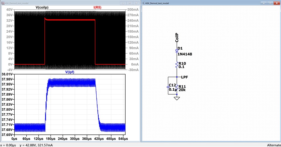
I have to design an asynchronous ASK demodulation circuit for one of my wireless charging projects, where the receiver data superimposed on transmitter voltage need to be demodulated by measuring the transmitter coil voltage. I am also attaching the simulation results of transmitter coil voltage and receiver data in the upper waveform, which shows a slight variation in the voltage amplitude. This voltage is then given to an envelope detector followed by low pass filter, which shows nearly 300mV difference in voltage from its nominal value (below figure). To further decode this signal, I need to design an amplifier circuitry along with other filtering that can provide sufficient amplitude level. I tried to search the amplifier OpAmp IC and got "OPA2383".

Thus, I wanted to ask if the selected IC is good one for my application if not what is the alternative IC I can use. Also, I wanted to design suitable filtering circuit for the amplifier circuit, and I am a newcomer in this field, thus is there any available tool which I can directly adopt to design the amplifier that you can suggest. It would be a great help!

Regard

Vivek

  • Vivek,

    It is too ambiguous to say “…the circuit should provide… sufficient amplitude level.” Thus, in order to assist you, please specify using numbers the required precision (offset voltage and temperature drift), speed (bandwidth), gain and maximum noise.  Also, it would be very helpful to show proposed circuit schematic of the demodulation circuit including values of the components.

  • Hi Marek,

    Thanks for your reply. The used below link to get the information related to demodulation circuit on page 5.

    AN4701, Demodulating Communication Signals of Qi-Compliant Low-Power Wireless Charger Using MC56F8006 DSC - Application Notes

    Talking about the actual numbers of (offset voltage and temperature drift, bandwidth) required for precision so I am not sure about it as it is new for me. But the required gain is nearly 11 because I want logic level output (3.3V) from the output of low pass filter (nearly 300mV, you can check the waveform I provided earlier). Also, the maximum noise should be nearly 100mV. As I am new in the analog circuit designing, I request you to help me in designing the complete demodulation circuit or provide some document that can help me to understand and design the demodulation circuit.

    Regards

    Vivek

  • Vivek,

    I can help you with some of the circuit but I cannot design your entire demodulation module - if we were to do it for all of our customers, we would need an army of engineers.

    Since the voltage step down circuit is AC coupled, there is probably no need for precision like OPA2383 zero-drift amplifier so TLV9052 or OPA2392 should be good enough. As far as the gain goes, it cannot drive the output to its rails so differential input of 300mVpp could at most be gain by 10 (see AOL test conditions).

    In the case of 10 to 1 front-end voltage divider (20k/200k - see VM1), Vcoil of 20Vpp translates into VM1 of +/-200mV, which in turn results in the output, VF1 = Vref +/-1V = 1.65V+/-1V -  see below. 

    Below I have attached Tina-TI schematic for your own simulations. 

    You may download a free copy of Tina-TI by clicking on the following link:  https://www.ti.com/tool/TINA-TI

    TLV9052 Voltage Scale Down circuit.TSC