This thread has been locked.

If you have a related question, please click the "Ask a related question" button in the top right corner. The newly created question will be automatically linked to this question.

OPA855DSGEVM: Current flowing In+ node in testing OPA855DSGEVM

Part Number: OPA855DSGEVM
Other Parts Discussed in Thread: OPA855

Tool/software:

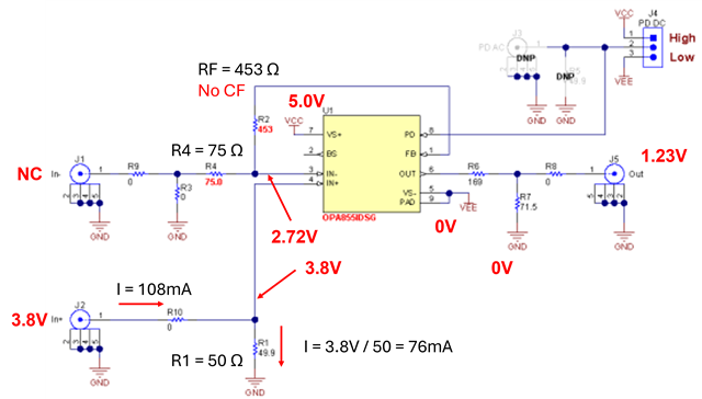
I am testing OPA855DSGEVM as TIA presented in the OPA855 datasheet.

Supply voltages are connected in single-supply mode, VCC is set to 5V positive supply voltage, and VEE and GND are connected together to negative supply voltage from a supply voltage generator.

In+ node is set to 3.8V as shown in Figure-9.1 in OPA855 datasheet and In- is not connected yet.

While supply generator is turned on to supply VCC and In+ node voltages (Vcm), I am seeing large amount of current (~108mA) through In+ node and 28mA at VCC node reading from the supply voltage generator.

Is this 108mA current expected from In- node under these supply voltages?

  • Hi Doo,

    Can you probe the output and check if the device is stable or not. Do you see any oscillation at the output?

    Regards

    Anant

  • Hi Anant,

    Thank you for your reply.

    I thins the current (108mA) flowing IN+ node is mostly coming from 50 ohm (R1), 3.8V / 50ohm=76mA and +10mA of input current to bipolar type amplifier. Please correct me if I am wrong.

    Here are what I am seeing the voltage waveforms from interested nodes (out, IN-). I don't see any oscillation at the output.

    Are these voltages (IN- and OUT) expected under this condition (Vcc = 5V, Vee=GND=0V)?

  • Hi Doo,

    10mA of current will not go into the IN+ node under normal operation, than max input bias pin from IN+ is <20uA at room temp.

    Your total gain in this case is 7V/V and input is 3.8V. So your device output will try to go to 3.8x7 = 26V. And therefore it will rail to positive supply. Since the supply is 5V and the max output swing it can go is ~0.9V below Vcc (see the VOH of datasheet electrical table) so the output will be clamped at 4.1V. That is why you are seeing 1.23V at the J5 after attenuation from R6 and R7. This will cause the device to go out of the closeloop configuration.

    If you want to test it in TIA configuration, you need to remove R3 and change R4 to 0 ohm, but it that case you have to connect the photodiode also and you might also need to put Cf based on your photodiode capacitance.

    If you just want to test it as a gain amplifier at 3.8V common mode ( at 5V single ended supply) you need to remove R3 and have to give 3.8V at J1 also.

    Regards
    Anant 

  • Hi Anant,

    When I changed the supply configuration to single supply, I can see the current at IN+ node looks fine.

    In my project, I am using a laser diode generating short pulse (1~2n sec) and my APD has min of BW at 1Ghz to receive this short laser pulse. So I choose OPA855 amplifier having high GBWP to use as TIA.

    Like you suggested, I updated the schematic of EVM board in TIA configuration.

    1. Use split supply configuration (Vcc = 2.5V and Vee = -2.5V and GND = 0V)

    2. Remove J1 SMA, remove R3, change R4 to 0ohm,

    3. Put Cf (0.4pF) on the top of R2 resistor using the values from TIA calculator since APD capacitance is 1.5pF from its datasheet.

    Q1. Please review the image above showing the schematic using OPA855 as TIA.

    Q2. I see R6 and R7 is working as voltage divider having 0.3V/V gain. Can I remove these resistor and just connect J5 to oscilloscope to monitor the voltage output?

    Q3. Since we are using split supply configuration, can I set J2, the input common mode to gnd? Also is it okay to remove R1?

  • Doo,

    Schmatic looks fine. 

    R6 and R7 are there to isolate any paracitic capacitance of the load connected at J5 and the same time it's parallel equivaent is 50ohm so if you connect scope with 50ohm termination it will match the impedance and hence will reduce the signal reflection. Removing it all  togeather can make the amplifier unstable. So if you want to reduce the attenuation, you can remove R7 and connect 50ohm at R6. Configure your scope with 50ohm termination (input impedance) and connect the J5 to scope with a sma cable with has controlled impedance of 50ohm.

    Yes R1 can be removed and the input common mode can be set to gnd here but to get the maximum input range you should bias it at around 1V below VCC (1.5V in yor case). 

    Regards

    Anant

  • I modified this OPA855 EVM to TIA configuration by removing R3 and shorting R4 (No feedback capacitor Cf is connected yet). I also removed a SMA connector at IN-. Anode of APD is connected at In- but Cathode is open.

    In the image below, the outputs measured at output of U1 and J5 from the oscilloscope are shown when 1V is applied to J2 (1.5V below Vcc).

    I can see 1V voltages are measured at pos and neg inputs of U1. But I am seeing oscillations around 1V at 'out' node of U1 and 0.3V at 'Out' from J5).

    How can I remove this oscillation at outputs? Should I put feedback Cf capacitor (0.3p~0.5pF) obtained from TIA calculator? (Required parameters are given to the calculator to get Cf value).

  • Hi Doo,

    If you don't bias the APD, the device OPA855 will actually be in a gain of 1V/V. And at this gain the opamp will be be stable it need a minimum gain of 7V/V. So you need to properly bias the APD it, and based on the paracitic capacitance at the In- (APC capacitance + trace paracitic capacitance), you may need to put a feedback capacitance in order to make it stable.

    Regards

    Anant