This thread has been locked.

If you have a related question, please click the "Ask a related question" button in the top right corner. The newly created question will be automatically linked to this question.

OPA551: Assessing phase margin for driving a piezo transducer load

Part Number: OPA551

Tool/software:

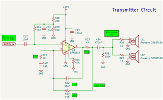
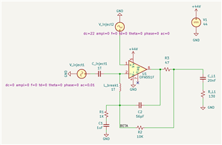
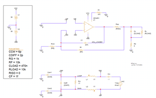
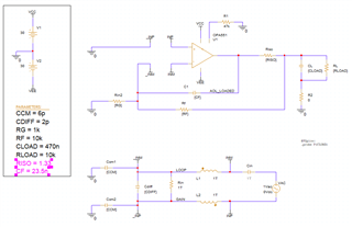
Hello, I'm working on a design to drive two piezo transducers in parallel using an OPA551. I've been trying to assess phase margin using a "break the loop" method in SPICE to ensure it will remain stable with the highly reactive load, and I'm having problems getting to a sane result. Attached is my actual circuit, and then my simulation circuit where I'm attempting to break the loop for AC analysis. I believe the analysis suggests 85 degrees phase margin, however if I increase the load capacitance to a ridiculous value like 10uF, it remains the same, so I believe my sim circuit is wrong. Can I please have some assistance assessing phase margin for this circuit, and also feedback on why my simulation circuit is incorrect? I'd like to use it to assess the best isolation resistor value to use. I have watched a couple of TI videos on the topic but am still struggling to get a simulation result that makes sense to me over various Riso and load conditions.

  • Hi David, 

    Apologies for the late response as we come back from 4th of July Holiday. 

    The problem with the circuit analysis is not your analysis method but instead the snubber circuit at the end of the analysis.
    Snubber circuits (C_L1/C24 & R_L1/R25) are notorious for stability simulation analysis; these are better suited for 'guess and check method' in theory/lab applications. 

    I have a file I created in PSpice for TI that can be reused for a variety of stability analysis, it follows the teachings in this video: Breaking loop on differential amplifier | Video | TI.com

    Here is the file: non-inverting-2025-07-07T20-03.zip

    I would remove the AC coupled caps for the stability analysis and change the power supply to be the max dual supply to help the model with convergence. Here is my circuit, notice how I made the resistor in the snubber nonexistent (0 ohm): 

    The resulting phase margin is 12 degrees: 

    I have also included post processing formulas that suggest an RISO & CF to achieve adequate phase margin: 

    RISO:

    First value is typical, second value is more conservative - the tradeoff is larger number has greater inaccuracies at larger current but higher phase margin.

    CF: 

    First value is typical, second value is more conservative - the tradeoff is larger number has slower settling time but higher phase margin.

    I changed the RISO to a 1% typical value of 1.33 & CF to 23.5nF: 

    The corresponding phase margin is 53 degrees. 

    When I use the R in the snubber circuit - it also provides inconsistent results. 

    All the best,
    Carolina

  • Hi Carolina,

    Tthank you very much for the detailed explanation, reference simulation circuit, and stability results. Regarding the suggested RISO and CF values, I believe the very large CF value greatly limits the bandwidth of the feedback loop and does not keep my frequencies of interest (30kHz-40kHz) at the desired gain level. However, I've been able to reproduce these results in simulation now, and I can use this as a basis with a more representative load to tune my circuit accordingly.

    Very best,
    David