This thread has been locked.

If you have a related question, please click the "Ask a related question" button in the top right corner. The newly created question will be automatically linked to this question.

INA129: Abnormal Supply Current in INA129U

Part Number: INA129

Tool/software:

We are encountering an issue with the INA129U components received in our most recent order.

When assembled in our circuit, these components draw approximately 0.2 mA of supply current.
In contrast, INA129U components from previous orders, when mounted on the same circuit and the exact same PCB, consistently draw only 0.05 mA under identical operating conditions.

We have been using the INA129U for over five years in this exact application, on the same PCB and circuit configuration. Only the components from the most recent batch exhibit an increased supply current of ~2 mA. This deviation causes our product to fail under standard operating conditions.


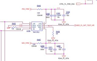
Please find the application schematic attached.

https://postimg.cc/NKVhCR9X

Best regards.

  • Hello Roman,

    I believe I have been shared the schematic (I am unable to access the link you have posted due to an internal firewall). Please let me know if the below is correct. Additionally I have a few questions:

    1. do you know what voltage is present on IN+, IN- and OUT when the supply current is increased?
    2. What is providing the input to the INA129?
    3. Is there an RC filter on pin6 of the device?
      1. If so, could you please share the values of these components?

    Best,
    Gerasimos

  • Hi Roman,

    Would you be able to share the LOT# / date code ? or a picture of the sticker on the reel ?

    Regards,

    Nir

  • Yes, the schematic is correct.

    Yes, the schematic is correct.
    I would like to clarify that the supply current consumption of the INA129U from the recent batch is approximately 2mA, not as initially mentioned in my first message.

    Below are the answers to your questions along with additional operational details:

    1. IN+ is connected to a voltage output ranging between 18V and 20VUnder normal operation (when no resistance measurement is being performed), the INA129U IN+ pin is floating.When IN+ is briefly connected to the supply voltage, this is when the increased current consumption occurs, which I referred to earlier.
    When i attuch INA129U from privios batch on the same circuit and the exact same PCB, consistently draw only 0.05 mA 

    IN− is connected to P24V_FL_RTN (power supply ground) via a fixed 1kΩ resistor.

    An additional resistor — which is the target of the resistance measurement — is connected between pin 3 (IN+) and pin 2 (IN−) of the INA129U.
    This resistor typically has a value of 10kΩ.

    However, during the resistance measurement, the IN+ pin is disconnected from the voltage source (left floating), so it is not exposed to the 18V–20V supply voltage during the measurement.
    When a command is received, a current of approximately 200mA briefly flows through the measured resistor (current source: REF200AU), allowing the system to perform a single-point (momentary) resistance measurement based on the voltage drop between the INA129U input pins

    2.The input to the INA129U is provided by a Traco DC-DC converter: TRS 2-2421 (+/−5V, 2W).
    3.There is no RC filter connected to pin 6 of the device.

  • Hey Roman,

    Sorry for the delay here. I would like to clarify some details about the application.

    1. The INA129 is supplied with +/-5V supplies, but the input voltage at IN+ is 18-20V?
      1. In this mode, are you expecting linear operation out of the INA129?
    2. The increased current consumption is seen when the input voltage is connected to the supply voltage, is that V+ or V-?
    3. Is the increased current measured sourced from V+ or sunk into V-?

    Best,
    Gerasimos

  • Thank you for your response.
    Let me clarify the application and address your questions point by point:

    1. Power Supply and Input Voltage:
      Yes, the INA129 is powered with ±5V supplies.
      However, the input voltage at IN+ (during certain conditions) is briefly connected to a high-side voltage of 18–20V through a resistor. This is not a continuous connection — it occurs for a very short duration and only outside of the actual resistance measurement.
      During the measurement itself, IN+ is left floating (disconnected from the 18–20V supply).
    2. Expected Operation Mode:
      We do not expect linear operation of the INA129 during the brief moment where 18–20V is present at IN+.
      The actual measurement is performed only when IN+ is floating, and the measured resistor is placed between IN+ and IN−. The INA129 is then expected to operate linearly within its normal input common-mode range during the measurement phase.
    3. Increased Current Consumption:
      Yes, the increased current consumption (~2mA) is observed when IN+ is connected to the 18–20V supply for a short moment.
      We are currently investigating whether the excessive current is being sourced from V+ or sunk into V−, but based on our current observations, it seems that the device is drawing additional current from V+ during this brief connection to high voltage.
      In contrast, INA129U components from previous orders, when mounted on the same circuit and the exact same PCB, consistently draw only 0.05 mA under identical operating conditions.
  • date code: 2320

    LOT: 3391085ML3

  • Hey Roman,

    What is the duration of the input overvoltage?

    There was a qualification of an additional design in 2022. Here is the PCN that was provided to digikey. You should have been provided this information from TI if purchasing directly through us, or through a distributor if purchasing through another channel.

    https://mm.digikey.com/Volume0/opasdata/d220001/medias/docus/5340/PCN20220802000.1.pdf

    My first hunch is perhaps a difference in the speed of the input overvoltage protection. I will reach out to the design team to confirm of any differences between the original design and the new design.

    Best,
    Gerasimos

  • Thank you for your response.

    Under normal operation, the input overvoltage duration is very brief — typically just a few milliseconds when IN+ is momentarily connected to the 18–20V source outside of the actual resistance measurement window. During measurement, IN+ is floating and not exposed to the high voltage.

    However, during our investigation of the increased supply current, we intentionally applied the 18–20V input voltage for a prolonged period — several seconds — in order to reproduce and analyze the behavior. 
    During our investigation, we observed that the increased supply current persisted throughout the entire duration of the test, while the input voltage (18–20V) was applied to IN+ for several seconds.

    We appreciate your support and look forward to your update from the design team regarding any changes to the input protection circuitry.

  • Hey Roman,

    Are you able to test the devices with the expected performance with the same sustained overvoltage condition? This will help narrow down if it is the speed of the OVP circuitry, or if there is a different implementation.

    Best,
    Gerasimos