This thread has been locked.

If you have a related question, please click the "Ask a related question" button in the top right corner. The newly created question will be automatically linked to this question.

LM393LV-Q1: open-drain output question

Part Number: LM393LV-Q1
Other Parts Discussed in Thread: LM393LV, SN74AHC1G00

Tool/software:

Hi,

I've been having a problem lately with comparator of LM393LV.

When the pull-up resistance is too high, port voltage of the comparator is abnormal, port voltage is 0.

I wonder if this phenomenon is related to the pull-up resistor being too large.

Thanks.

  • Hello Eric,

    There is a small internal leakage that is temperature dependent. Contamination on circuit board adds to leakage. Measuring the output voltage can also be a leakage current.

    pull-up resistor being too large.

    How large doesn't work and what value does work?

    Do you have a schematic to share?

  • Thanks, Ron

    Schematic is shown below:

    First problem is the absence of filter capacitance.

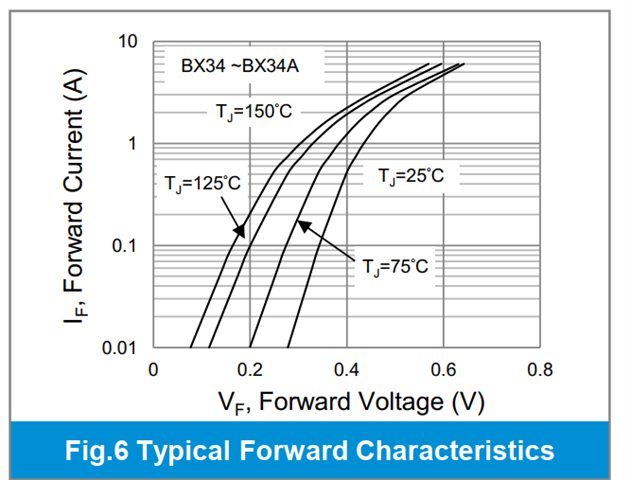
    Secondly, The selection of diode D1 is wrong.The parameters of the diode are shown in the figure below.

    What I want to know is, does this pull-up problem can cause problems with the input pins, such as threshold voltage deviation from the set value.

  • Add, The missing filter capacitor has been added to the board. Problems still arise

  • Eric,

    R1 is a pull up and R9 weak is a pull to pin 5 resistor.

    Where was this abnormal 0 V observed? What are voltages at at purple nodes. What load is at Cout node (where does it go)?

  • When problem arises,

    1. 0 V is observed at Pin 2,3,5,6.

    2. C_IV is 1.65V, Pin 7 is 0V

    3. C_out connects SN74AHC1G00

  • Eric,

    Assuming the reported measurements and schematic are correct the following has to be true. Pins 2,3,5,6 are damaged, shorted to pin 4 (ground). This would be a permanent condition. So some samples would work fine and others are damaged and do not work at all.

    The original report suggest that the value of R1 affects all samples, good or damaged.

    C_out connects SN74AHC1G00

    If output only goes to input of this chip and all supplies are 3.3V , then what is the purpose of D1? It seems to be not needed to me. 

    Is this a new or old design? What is the failure rate?

  • Hi,Ron

    It's a new design, and this problem only appears on one board.

    Since it is an individual problem, I prefer to believe that other factors are responsible, such as PCB process problems.

    I'll continue to analyze the reasons. This question will be temporarily closed.

    Thank you for your help.