Tool/software:
Dear team,
Could you please tell me why add VCM clamp FET for new chip?
I look at the materials below.
https://www.ti.com/jp/lit/an/snoaa35f/snoaa35f.pdf
Best Regards,
Seijiro Matsuoka
This thread has been locked.
If you have a related question, please click the "Ask a related question" button in the top right corner. The newly created question will be automatically linked to this question.
Tool/software:
Dear team,
Could you please tell me why add VCM clamp FET for new chip?
I look at the materials below.
https://www.ti.com/jp/lit/an/snoaa35f/snoaa35f.pdf
Best Regards,
Seijiro Matsuoka
Hello Matsuoka-san,
See sections 6.2 and 6.3 of that appnote.
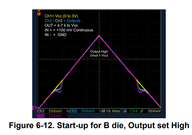
The original die output went *low* when *both* inputs are above VCM.
The first PCN die added an extra gain stage (Q13/14), which added an inversion to the signal path.
However, this inversion caused the output to go *high* when both inputs are above VCM.
Many customers designs relied on the output going low and caused many issues.
The second PCN added the Q15 clamp to mimic the original device behavior (output low) when *both* inputs are above VCM.
Q15 is normally out-of-the-circuit until both inputs are taken above VCM and cut-off the input stage (no tail current). When this happens, Q15 conducts and forces the output to go low - mimicking the original device behavior.
Grohe,
Thank you for your explain.
Let me check if my understanding is correct.
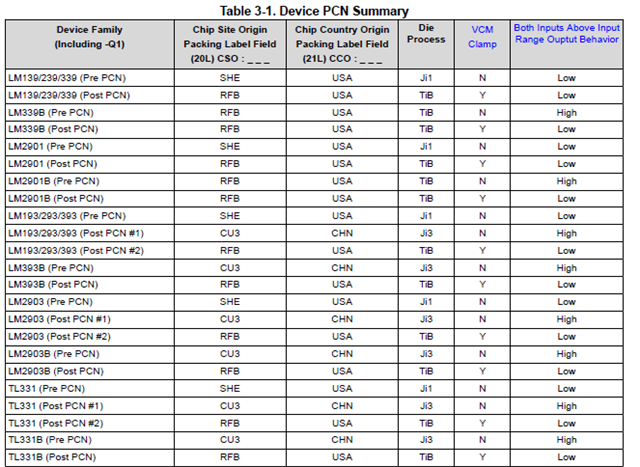
Is the following the correct behavior for each Die?
Also, what does VCM mean?
Behavior of LM2903B (Pre PCN)
it's High.

Behavior of LM2903B (Post PCN)
it's Low.

Best Regards,
Seijiro Matsuoka
Hello Seijiro,
Your understanding is correct.
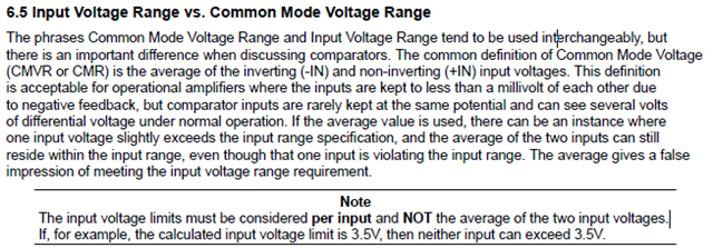
"VCM" means "Voltage Common Mode". This is more associated with op-amps, but it is the voltage on the input pins.
This is explained in section 6.5 of the application note: (CMVR and VCM are interchangeable).

Table 3.1 shows the behavior differences between the dies:

Remember, this behavior ONLY happens when BOTH inputs are above the input limit.
For example, the input range limit is Vcc-2V, or 3V input max on a 5V supply.
If the input voltages on BOTH input pins are simultaneously above 3V, the output state will be as noted in the "Both Inputs Above Input Range Output Behavior" column for that die revision.