This thread has been locked.

If you have a related question, please click the "Ask a related question" button in the top right corner. The newly created question will be automatically linked to this question.

TLV7031: Comparator configuration

Part Number: TLV7031
Other Parts Discussed in Thread: TLV1831

Tool/software:

Dear Team ,

My circuit and it's output wave-from is given below.

The green color is the output waveform. The amplitude varies from 0 to 2.1V.

This output will be given to a comparator and at the comparator output also I need the same green signal.

Actully for making it clean we are proving it to a comparator.

Below is the initial comparator circuit.

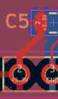
The comparator output currently I am getting is zero.Below is my board file

I tried to simulate the comparator using Tina TI.The circuit shown in the board is given below.

It is working in simulation but not in board.May I know where I went wrong.In the simulation you can see comparator output ramping from zero.

The signal data rate is UART 9600

COMP_Closedloop.TSC

Do I need to move to open loop.

Comp_Openloop.TSC

Regards

HARI

  • Hi Hari,

    I do not see an issue with the comparator circuit as drawn.

    Have you probed the comparator pins to make sure that the supply and reference voltages are present *AT* the comparator pins? Checked for shorts?

    Does the output move at all? If you change or remove the reference voltage?

    Made sure that the correct device is installed? Verified the resistor values?

    I would make ground traces a little thicker...reduce inductance that will reduce ringing. The TLV1831 should be treated as a high speed digital device.

  • Hi Paul,

    Thank you very much.

    I will check the board again and will update you.

    I would make ground traces a little thicker.

    Could you please suggest a value.This is my 1st proto,I can take care in my second revision.

    Regards

    HARI

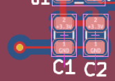
  • I usually make them at least a mil or so smaller than the pad, or the width of the via pad.

    You had it about right here...

    I would make the bottom GND trace the same width as the top traces:

    You could also thicken the trace width to the diameter of the via annular ring..and maybe move the via a little closer.

  • Hi Paul,

    You are right,after providing a touch up for comparator section,the board is working fine now.

    May be some dry solder or something.

    Actually we are doing an experiment.Discrete implementation of this IC.

    Thank God,it is working in the lower speeds.I believe if I use Opamps with GBW greater than or equal to 1Ghz.The circuit will work for higher speeds also.

    Regards

    HARI