This thread has been locked.

If you have a related question, please click the "Ask a related question" button in the top right corner. The newly created question will be automatically linked to this question.

TPS16850 and INA745B: Implementation Query

Part Number: INA745B
Other Parts Discussed in Thread: INA260, TPS1685

Tool/software:

I am using the TPS16850VMAR (eFUSE) and INA745BIRELR (current monitor) in a 28V power path, where the 28V is referenced to a noisy power ground. The INA745BIRELR is intended to monitor the power flow of the 28V line.

My concern is regarding the INA745BIRELR: since its operating supply voltage (VS) is 2.7V to 5.5V, we are supplying it with 3.3V (as shown in the attached schematic). However, the 3.3V ground reference is different from the 28V power ground being measured.

Could you please confirm if this configuration could cause any functional issues? Is this an acceptable way of implementation?

Additionally, kindly review both the eFUSE and VI monitor circuit diagrams and let me know if the implementation is proper, especially with respect to the resistor values matching the table configurations.

Appreciate your feedback.
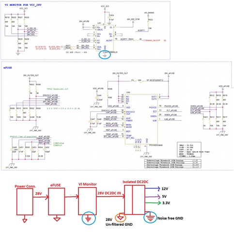
Regards,
Anoop

  • Hi Anoop,

    Our device will need to be on the same ground as the load (the noisy ground). We have a reference design about how to do this using the INA260 (integrated shunt) along with a digital isolator. https://www.ti.com/tool/TIDA-01608 

    As for the EFUSE I am going to pass you off to the team that handles that.

    Best,

    Holly

  • Hi Anoop,

    I will check and get back ASAP. 

    Regards

    Kunal Goel

  • Hi Kunal,

    Thank you for your response.
    Waiting for your feedback on the eFUSE schematic to proceed further.

    Best regards,
    Anoop

  • Hi Anoop,

    1. Please add 22pF on temp pin and remove the resistor if you are using Temp pin.

    2. Please add ceramic decoupling cap on VIN and VOUT pins. 

    3. Schottky diode recommended on VOUT pin.

    FYI,

    TPS1685 IMON pin also offers precise current monitoring.

    Regards

    Kunal Goel

  • Hi Kunal,

    Thank you for your feedback.

    1. Regarding the TEMP functionality—if it is not being used, can it be pulled down to GND using a 10kΩ resistor? This is intended to avoid any potential noise coupling through the pin if left unconnected. Please confirm if this approach is appropriate.

    2. The suggested changes will be incorporated as per your recommendation.

    3. We are currently using a P-Channel MOSFET on the VOUT pin for output control from the eFUSE (not shown in the schematic). Could you confirm whether this is acceptable, or if a Schottky diode is mandatory in this case?

    For the IMON pin, it is being used solely to configure the maximum current limit setting. Kindly confirm if this implementation is valid.

    Looking forward to your confirmation.

    Regards,
    Anoop

  • Hi Anoop,

    I will get back before tomorrow EOD.

    Regards

    Kunal Goel

    1. Regarding the TEMP functionality—if it is not being used, can it be pulled down to GND using a 10kΩ resistor? This is intended to avoid any potential noise coupling through the pin if left unconnected. Please confirm if this approach is appropriate.

      Should be fine . Leaving open is also fine as device does not take any action based on TEMP pin data.

    2. The suggested changes will be incorporated as per your recommendation.

      OK

    3. We are currently using a P-Channel MOSFET on the VOUT pin for output control from the eFUSE (not shown in the schematic). Could you confirm whether this is acceptable, or if a Schottky diode is mandatory in this case?

      P-channel mosfet. Should be fine

    For the IMON pin, it is being used solely to configure the maximum current limit setting. Kindly confirm if this implementation is valid.

    Yes it is fine. IMON pin voltage can be used for current monitoring also.

  • Hi Kunal,

    Thank you for your feedback. Based on your input, I’ve finalized the schematic.
    Appreciate your support throughout the process.

    Have a great day!

    Regards,
    Anoop

  • Hi Kunal,

    Additionally, regarding the TPS1685 implementation — the PGOOD, FLT, and SWEN pins are connected to the 28V rail via voltage dividers, which bring the voltage down to 5V at the IC pin side. Could you kindly confirm whether this approach is acceptable?

    Please refer to the schematic I previously shared and let me know if any corrections are needed.

    Thanks and regards,
    Anoop

  • Hi Anoop, 

    This should be fine .

    Regards 

    Kunal Goel