Other Parts Discussed in Thread: TPA3116D2
Tool/software:
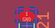
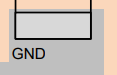
 Class D Amplifier.pdfHello, I am looking for an overall schematic and potentially a PCB review (although the PCB is not complete and I am a total beginner when it comes to schematic and PCB production), specifically ensuring proper implementation and component values of the TPS611781. My overall project is an ESP32-controlled bluetooth speaker. For the project, I am powering the circuit with a 3S2P configured lithium ion battery pack producing about 12V. However, to get louder performance out of the TPA3116D2, I wanted to boost the voltage to around 20V. To do this, I decided to use the TPS611781 as its switching frequency can be configured well above the frequency range of the audio spectrum, and does not require many extra parts. I am not sure however that I chose correct values for components, so I would like that checked. Finally, I was wondering how grounds should be layed out on my PCB. I saw on the datasheet that power ground and analog ground should be connected only at one point, so I decided to have a copper layer on the top and bottom layer for analog ground which provides ground for the TPA3116 amplifier and some pins of the TPS611781 as outlined from the datasheet, and then another copper layer for power ground of the TPS611781 on the top and bottom layer. Finally, I included a net-tie to connect the grounds at a single point, but I wanted to know how I should actually make that connection on my PCB. Thanks for any help.