


Tool/software:
Hi guys,
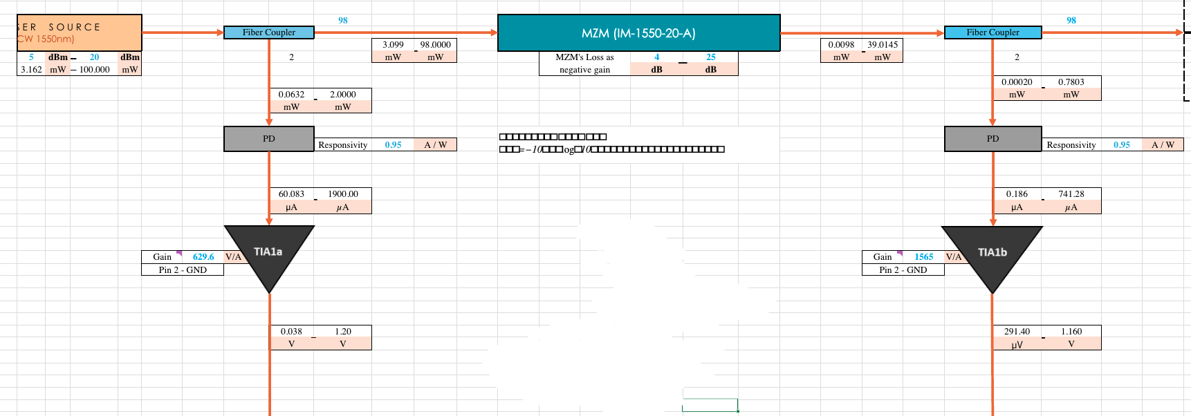
I've put in all the work I could hooking up the OPA857 to reverse biased Photodiodes with my beginner's experience in PCB Design and I need some expert's advice on my finished schematic. I've gone through majority of the threads in this forum to make necessary changes, now I need you guys to take a quick peek :) I've attached an excel file (power budget) pic that includes my calculations of how much current we might expect and a pic of the schematic.

I've also attached the photodiode datasheet for reference.
I've tried to reduce the gains of TIA to be able to input >240uA of photocurrent. (assuming it would swing from 0-1.2V) Also the CTRL pin is connected to GND, so the internal gain of TIA should be 5k
1. Is the output of OPA857 a positive voltage? (just wanted to confirm)
2. Can we connect resistor and cap like this from IN to OUT?
3. In datasheet schematic, there's a 25ohm resistor after the op-amp. Does that affect the gain? Or is it there to impedance match for RF?
