Tool/software:
Hello,
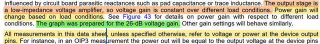
The datasheet specifies that all measurements refer to the device output pins unless otherwise stated.
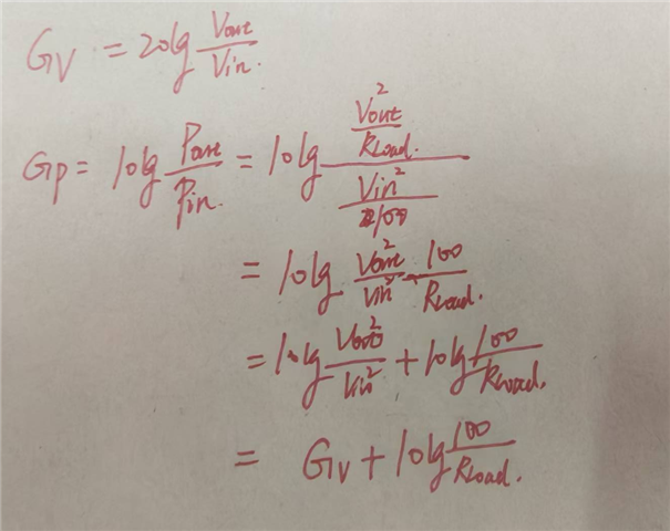
How should I interpret the power gain (Gp) calculation in Figure 43 when the voltage gain (Gv) is 26 dB?
When the load impedance at the output pins is 100 Ω, the power gain (Gp) equals the voltage gain (Gv) at 26 dB. However, the figure 43 displays it is 20dB.
Does the term 'Rload' here refer to the load directly at the device output pins?
Or does it represent two 50 Ω resistors connected differentially between the output pins and the external load?"
Thanks!