This thread has been locked.

If you have a related question, please click the "Ask a related question" button in the top right corner. The newly created question will be automatically linked to this question.

OPA855: DC Offset at Non-inverting terminal

Part Number: OPA855


Tool/software:

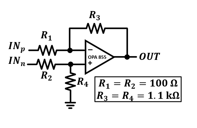
I wanted to use OPA855 to implement a wideband voltage subtractor from DC-100MHz. Here is the schematic that I use. The bias I use is VCC = 2.5V, VEE=-2.5V. I have added enough decoupling caps on VCC and VEE. When I powered it on, I saw that both INp and OUT have a DC value of -1.6V. INn has 0V DC. I plugged all INp, INn and OUT to the spectrum analyzer and did not see any tones (no oscillation). Could anyone help to debug the circuit?

  • Hello Boxun,

      When you power-on the OPA855 do you have INp and INn nodes grounded to same ground as R4?

    Thank you,
    Sima

  • Hi Sima,

    The INn terminal is has a DC path to ground by R4. The node INp has no DC path to ground. I assume the voltage is established using the virtual connection between inverting and non-inverting terminal given the large open-loop gain.

  • Hi Boxun,

    The device seems to be railing which usually means something is not biased correctly. Could you ground the INp node to ground as well. This should bias the circuit appropriately.

    Best Regards,

    Ignacio

  • Hi Ignacio,

    I tried to add a 100-Ohm resistor from the inverting terminal to GND. The DC current went to 80mA. I guess it turned on the ESD diode. I could not directly connect it to GND because this is a voltage subtractor which requires two inputs. 

  • Hi Boxun,

    Understood, can you share the schematic for your PCB. Any information about the prior stage will be helpful. Are you able to switch the unit? I am wondering if maybe the unit is damaged. If you have set a voltage at the inputs that would not violate the input/output range, then there is no reason this circuit would not work. This could mean the unit was damaged.

    Best Regards,

    Ignacio

  • Attached please find the schematic. I have changed the resistors to the following values (in Ohm):

    R1=100

    R2=1.1k

    R3=100

    R4=1.1k

    R7=0

    R8=open circuit

    The compensation capacitance C2 is left open.

    No oscillation is observed.

    Bias condition VCC=+2.5V, VEE=-2.5V, GND=0V.

  • Hello Boxun,

      I apology for missing a reply to your thread. The schematic looks correct, and R4 to ground will not violate the input when INP is not grounded. And, with INN (J1) not grounded it will look like a closed-loop buffer to the amplifier, and should work correctly to keep the voltage at close to 0V (small voltage offset specified in device datasheet). This most likely suggests what Ignacio mentioned earlier that the device might have been damaged. If replaced, let us know if that fixed the large DC offset issue.

    Thank you,
    Sima