This thread has been locked.

If you have a related question, please click the "Ask a related question" button in the top right corner. The newly created question will be automatically linked to this question.

LMC6042: stability of circuit

Part Number: LMC6042

Tool/software:

Hello,

I have a buffer design that I sometimes see instability on. This is actually installed in a product which we have a significant samples size of. Early builds do not easily show the instability, but the latest builds are more likely to become unstable.

After simulating the circuit in spice, i've found that the design is on the edge of acceptable phase margin, my question is why would some samples be more stable than others.  Is it process related? 

Here's the circuit.

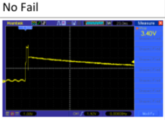
Here are actual in system results.

  • Hi Mattew, 

    i've found that the design is on the edge of acceptable phase margin, my question is why would some samples be more stable than others.  Is it process related? 

    C2, 200pF should not be present. That will degrade your phase margin significantly. C2 is placed pole before the unity gain BW of the buffer. If you do not want to change anything, then removed C2. 

    If you want to improve the performance and total noise of the circuit, you can try something below. 

    If you have other questions, please let us know. 

    Best,

    Raymond

  • Thank you. I agree with your assessment, but my question is regarding the why some units in the field do not exhibit the instability.   

    Would LM units on the cold side of the process be less susceptible?  If i was able to give you lot info (from markings) would be able to tell me where the devices i have reside in the distribution?   The reason for this question is that I am trying to reduce scrap rate of the product I have shipped and I need to determine the probability of failure.

    Regards,

    Matthew

  • Hi Matthew, 

    If i was able to give you lot info (from markings) would be able to tell me where the devices i have reside in the distribution? 

    There will some variances in BW and phase margin in different lots or ICs. From the No Fail plot, it is shown that there is significant overshoot, which means the phase margin is poor as it is configured. 

    In addition, this part does not have great phase margin to begin with at 0dB, and the phase margin can be degraded with small parasitic capacitive load. 

    So the phase margin in the circuit is very marginal and sensitive to the output parasitic capacitance (~50pF). With variations in different ICs, phase margins are operating right on the edge ~45 degrees (and also it changes with temperature). For these reasons, I think that this part should have compensated more per the application, since the circuit is operating at very low frequency. 

    If you have other questions, please let me know. 

    Best,

    Raymond