


Other Parts Discussed in Thread: AMC3330
Tool/software:
Hi all,
2 and 3 of J2 of AMC3330 were shorted and tested referring to the following data sheet.

"7.3 Best Design Practices
Connect the high-side ground (HGND) to INN, either directly or through a resistive path. A DC current path
between INN and HGND is required to define the input common-mode voltage. Take care not to exceed the input common-mode range as specified in the Recommended Operating Conditions table."
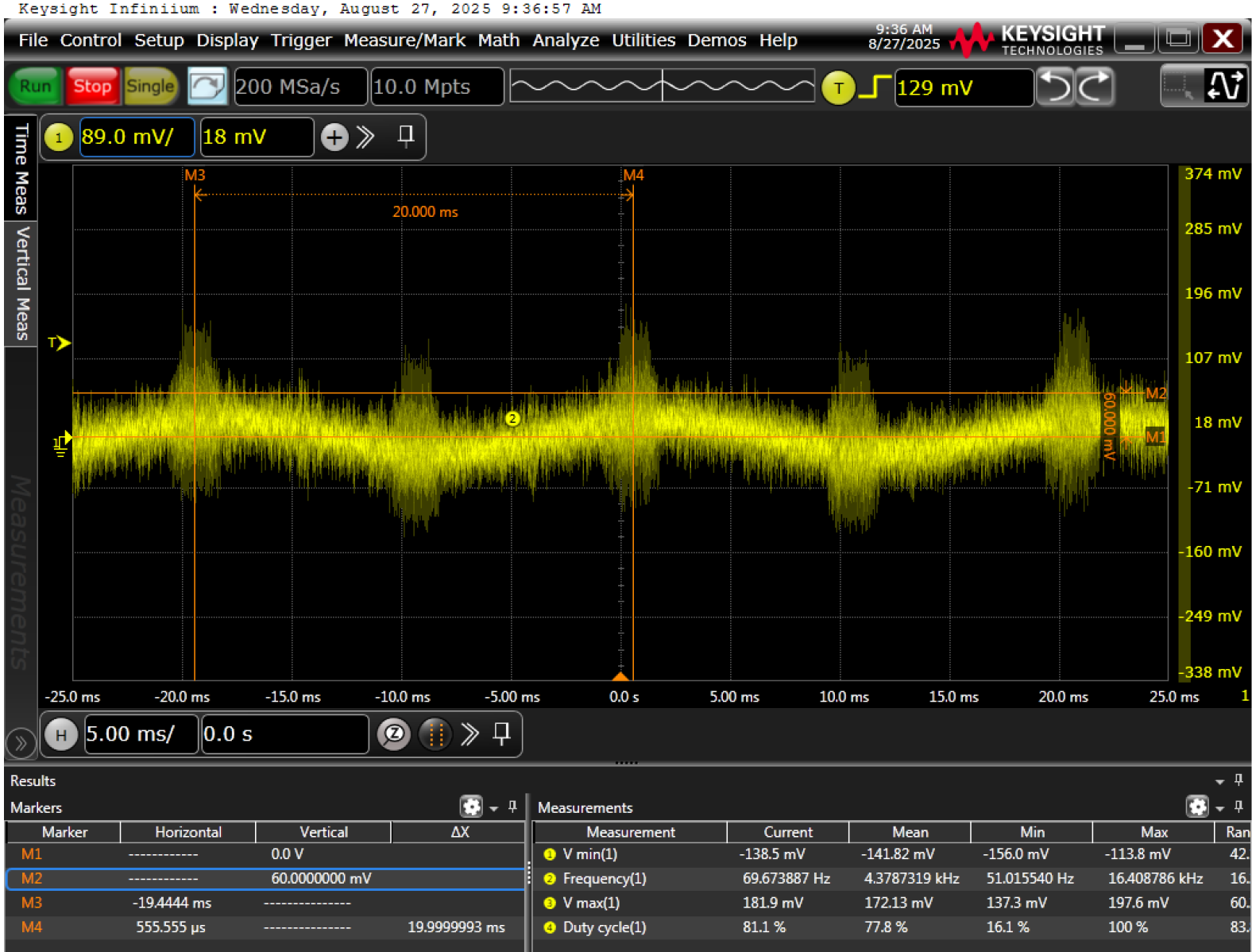
1Vp-0 waveform was designed between INP and INN as an input signal, and Pins 1 and 2 were measured with a differential probe.
However, only 60mVp-0 was actually observed.
What measures and settings are necessary to correctly measure the waveform of 1 Vp-0?
Do you know the cause?
In addition, when pins 1 and 2 of J3 were measured with a differential probe, the output waveform was 2Vp-0, which was as designed.
The circuit diagram, conditions, and waveform are shown below.
Input voltage: AC5Vp-0
Pins 1 and 2 were measured with a differential probe.

Best Regards,
Ryusuke


