This thread has been locked.

If you have a related question, please click the "Ask a related question" button in the top right corner. The newly created question will be automatically linked to this question.

TLV3601: Latch comparator

Part Number: TLV3601
Other Parts Discussed in Thread: TLV3603, TLV9022L

Tool/software:


Dear Everyone, 

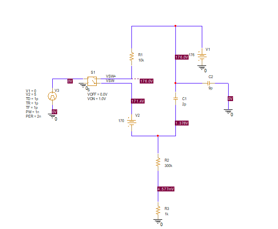
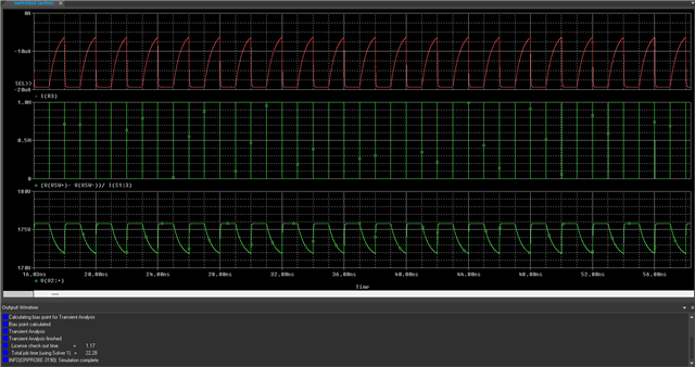
   Who can solve my issue . It seems that the switch doesn’t work fine if the input pulse is set in the nanosecond range. How can I change the settings in Options so that the switch operates correctly in the ns range?”


2nd question, what is the TI comparator PN  has the Latch function as AD8561 


Thanks,
Peter 

  • Hi Peter,

    1. What's the issue with the switch? I've gone ahead and sent you a friend request. Could you please share with me your PSpice file through direct messages?

    2. Here are all the comparators in our portfolio with a latching function: Comparators product selection | TI.com. The TLV3603 has a latch functionality similar to the AD8561. Some notable differences are that the TLV3603 has different pinout and package as compared to the AD8561, and the latch signal is active low in the TLV3603 while the latch signal is active high in the AD8561.

    There are some other devices where the latching function behaves differently like the TLV9022L. Could you please let me know what your application is? It could help me suggest a more applicable device for your application.

  • to_DR_Paul.pptx

    This is the switch as I mentiond.   You can refer my attached PPT. 

    Thanks. 

  • Hi Peter,

    I don't see how the second plot is indicative of the switch not working. If you are using the correct model, the PSpice voltage-controlled switch has the switch resistance according to the following equation:

    In the second simulation, you are changing the control voltage pulse width such that it will take longer for your probed voltages to reach steady state.

  • Hi HO SIU, 

      Thanks for your advice. Did you try simulating it to prove it? The circuit is small, and drawing it doesn’t take much time. Could you please try it first to confirm that it’s correct as you mentioned?

     Thanks,
    Peter 


  • Hi Peter,

    Below is the circuit:

    Below is my simulation. The top plot is the switch resistance. You can see that it swings to my defined RON and ROFF (1Ω and 1MΩ). The bottom plot is your probed voltage. You can see that it settles with a low ripple (because your switching frequency is much higher) at around 0.2us.


    In the future, you can use trace expressions in your plots to directly plot things like resistance. It'll be more effective for debugging as you'll be able to see exactly what you're looking for.

  • Dear HO SIU, 

    To clarify my request: I’d like to see the response shown below when the input pulse has PW = 1 ns and PER = 2 ns. Alternatively, for TD = 0, TR = TF = 0.1 ns, PW = 0.8 ns, and PER = 2 ns, how should I set up the simulation to obtain the same result? 

    When the input is configured with PW in the microsecond range, the response operates correctly. However, when PW is reduced to the nanosecond range, the same result is not obtained.


    Do we need to set more options? Anyway, I already tried .OPTIONS RELTOL=1e-4 ABSTOL=1e-12 VNTOL=1e-6 METHOD=GEAR RSHUNT=1e12 GMIN=1e-12, but it still didn’t work.


    Regards,
    Peter 

  • Hi Peter,

    This circuit and simulation are lacking context. Could you please describe the goal of simulating this circuit? What is this circuit trying to model exactly?

    I'm a little confused as to why you expect the same circuit to have the same output response for different inputs. When you change the period of the pulse source, you are changing your switching frequency. The capacitors need to take time to charge, and you are no longer fully charging them before the switch changes state. That is why it takes time for your probed voltage to settle.

    The only way to get a similar response with the higher frequency input would be to lower the values of the energy storage elements in your circuit such that they fully charge and discharge during the duration of your 1ns pulse width. I lowered the values of the capacitors by a factor of 1000 an obtain the following result:

  • Dear HO SIU, 

    Thanks, I get your point. This is an APD (avalanche photodiode) model simulated while the device is operating in Geiger mode, so C1 and C2 cannot be changed, as they represent parasitic values inside the model. In case you need to design it for nanosecond operation, what are you going to do?.  

    Regards,
    Peter 

  • Hi Peter,

    I apologize, but I'm unable to assist you on photodiode modeling as that is beyond my expertise.