Other Parts Discussed in Thread: LMK04828, LMK04832EVM
Tool/software:
Dear Xilinx Team,
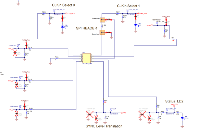
I am working with a CLK104 RF Clock Add-on Card (UG1437) and want to program it using TICS Pro via the TI USB2ANY interface.
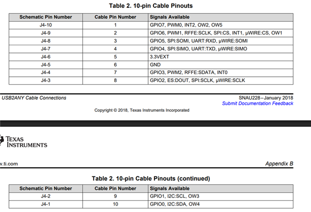
At present, I am wiring from USB2ANY (J4) → CLK104 (J33) with the following mapping:
- SDI: J33 (4th pin) → J4 (10th pin, SDA)
- SCL: J33 (8th pin) → J4 (9th pin, SCL)
- GND: J33 (6th pin) → J4 (6th pin, GND)
Could you please confirm:
- Whether the above wiring is correct for I²C communication between USB2ANY and CLK104?
Additionally, after performing the above wiring and attempting programming, I am not seeing the expected outputs at the ADC_REF_CLK_A/B and DAC_REF_CLK_A/B.

Any guidance or example configuration would be very helpful to validate whether this is a wiring issue or a configuration step I may have missed.
Your support and example references will help ensure correct setup before proceeding further with TICS Pro programming to CLK104.
Thank you,
Balu