Other Parts Discussed in Thread: OPA3S328
Tool/software:
Hello experts,
I have a design using the OPA2328 essentially as a "load isolating" voltage follower for a low drive-strength 15MSPS DAC, on account of it's good specs and the datasheet noting "Unity Gain stability". There was sadly no time to do EVK tests or a large-scale board, so we needed to go to a densely packed via-in-pad board design to have a chance at making the demonstration dead-line.
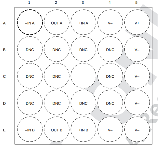
Now we see that if we feed a neat 500mVpp sine into "+IN A" on ball E1 and 500mVpp cosine into "+IN B" on ball E3 (measured on the feed-in resistor on the application board) then the "OUT A" on ball A2, routed straight through ball A1 ("-IN A") and on the "OUT B" on ball E2 routed out from the package and back to ball A3 ("-IN B") output a hard-clipped cosine output, swinging fully from 0V to 3.3V power rail and the sine is nowhere to be found.
On external optical inspection the alignment of the chips seems right: comparing to features it seems they are all placed so that their middle aligns with the "missing ball" in the footprint.
The Dot-mark on the chips comes out on the A1 ball on the footprint, which the datasheet definitely seems to strongly imply is correct (and also the only sensible way to stamp a BGA).
Me and my colleague cannot seem to find any errors in the design, directly comparing the board's footprint to the ballmap "top view" on page 4 of the datasheet:
https://www.ti.com/lit/ds/symlink/opa2328.pdf
The chip neatly gets 3.34V +/-20mV on various boards when the signals are applied (measured on the decoupling cap right next to the chip's A5 ball), which should be exactly in its operational range.
On the presumption I'm not the first ever person to use the DSBGA24 package to the OPA2328 I am thinking something went wrong in production.
We are also going to have an Xray inspection done, but that takes some time, so I thought I'd ask if there's any known production risks that might cause internal stress possibly causing this?
Is this package extra sensitive to high or long reflow peaks that may have been used due to via-in-pad reflow, for example?
I shortly considered it maybe being an OPA3S328 by accident, but the print on the chip really seems to say OPA2328. If it were an OPA3S328 that would explain it, because then:
The cosine goes into "+IN B"
The sine goes into "-IN B"
The output of amp B goes from "OUT B" to the output for the cosine channel, and into "+IN A"
And then "OUT A" routes through "-IN A" just like intended, making that output a voltage followed of the other output signal
Now, that wouldn't match the cosine input exactly in terms of phase, but at first sight it might look like it on an oscilloscope and both outputs would basiclly swing hard from V+ to V- on the sine/cosine intercept
But then a batch of OPA2328 would have to have actually been OPA3S328 that got mislabled. That seems weird to me. (although I would have strongly preferred the 3S328 pinout, because it's much eaier to route than the weird OPA2328 pinout).
Any thoughts welcomed while we wait for XRF scans.