LM2903: LM2903 Configuration

Part Number: LM2903
Other Parts Discussed in Thread: LM239

Tool/software:

Hi everyone,


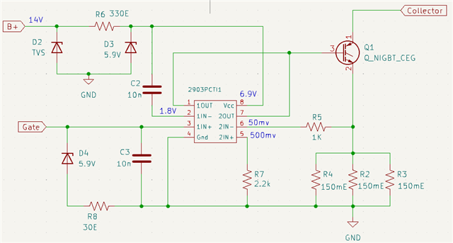
I recently bench marked a schematic used in a car ignition coil driver.

  • B+ → battery supply

  • Gate → input pulse from ECU

  • Collector → connected to ignition coil

The circuit works fine in the car, but I’m trying to fully understand how it operates.

The controller IC has the body marking “2903_PCTI1.” Since it mentions 2903, I assumed it might be similar to an LM2903 dual comparator. However, I’m not certain if it really is a comparator, or how exactly it’s being configured in this circuit.

Here’s what I observed during testing:

  • Under normal operation, the output signal follows the ECU’s gate signal, but the amplitude is limited to ~6 V.

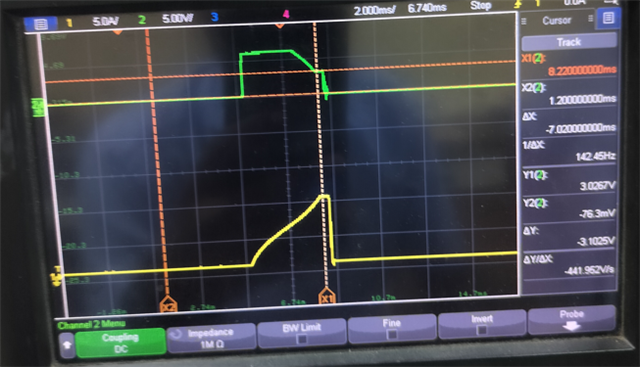
  • Once the ignition coil current (collector–emitter) reaches around 10 A, measured through a shunt resistor, the output amplitude gets clamped to ~3.3 V (waveform attached). CH2-Gate I/P to IGBT, CH1-Collector Current

  • I’m not sure how the circuit is implementing this amplitude limiting/clamping function.

If anyone can help me understand how this configuration works, it would really help me design a more optimized version for the same application.

  • Hello Ilavarasan,

    It looks like a LM2903 - but not a TI LM2903 as the markings do no match our marking style.

    I would double-check the circuit tracing. 

    My observations:

    1. There is no pull-up resistor on the output, unless the transistor has an internal pull-up resistor inside Q1. The comparator outputs can only ground the gate.

    2. There is no DC path to the IN1- pin (pin 2) - the 1.8V measured is probably the bias current across the meters 10M input impedance (assuming a 10M impedance 1.8V/10M=180nA - which is too high for the LM2903. A cap to Vcc makes no sense. Is there a divider hidden somewhere for the 1.8V. If it is truly floating, then it is a horrible design relying on going out of input range for the threshold.

    3. No bypass cap on the supply. That could cause false triggers due to a noisy supply. Could the bottom of C2 actually go to GND?

    4. 500mV on the 2IN+ does not make sense. It should be Ib*2.2k =  22nA*2.2k = 46uV. I there a 27k to VCC somewhere?

    What are you using to measure the voltages? Is it running when you are measuring? Then you may be measuring noise, as this is an electrically noisy environment.

    It looks like CH1 buffers the ECU gate signal, causing the CH1 output to go high (not conducting) when the Gate signal is high.

    The second channel output will go low when the 2IN- exceeds 500mV, which is when 500mV/50m = 10A is flowing through the shunt. So when the coil current is below 10A, the output goes high.

    Please note - we cannot give support on non-TI devices. Helping reverse-engineer existing commercial designs runs against TI policy. So you will have to investigate this on your own. Hopefully the above will give you some ideas where to start looking.

    If you have specific questions about a TI device, we will be glad to help.

  • Hello Paul Grohe,

    Thank you for sharing your observation. I understand that helping to reverse-engineer existing commercial designs goes against TI policy. However, I have been assigned to this project to develop our own solution. For that reason, I have decided to use the TI LM239 Quad Comparator for additional over-voltage and over-temperature protection. I benchmarked the existing design only to get an idea of how to get started.

    If possible, I would greatly appreciate guidance on building our own solution to meet the requirements. Specifically, I would like to know if it is possible to implement current limiting, over-voltage protection, and over-temperature cut-off using a comparator-based configuration.

    The schematic has already been reviewed by several people, but none of them were able to determine the exact configuration. There are no hidden components acting as voltage dividers for the CH1– and CH2+ threshold voltages. Measurements were taken using an oscilloscope with only the B+ (14 V) supply powered; no gate signal was applied. As you mentioned, when attempting measurements under running conditions, there is too much noise to obtain reliable results.