OPA547: Recommended land pattern

Part Number: OPA547

Tool/software:

Hi Team,

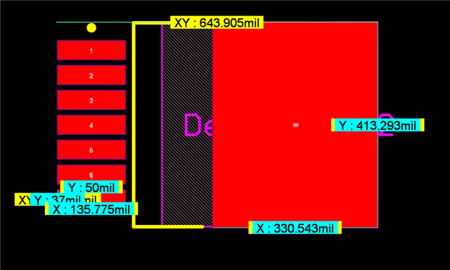
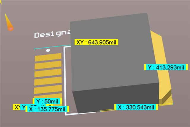
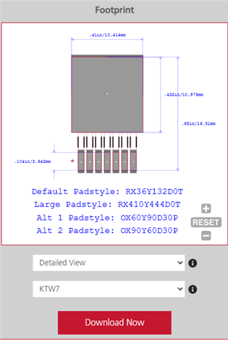
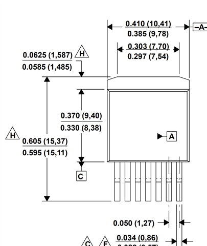
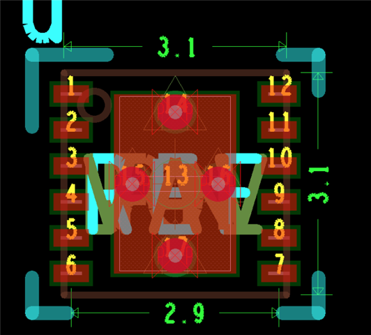
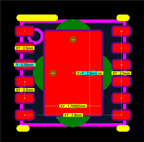
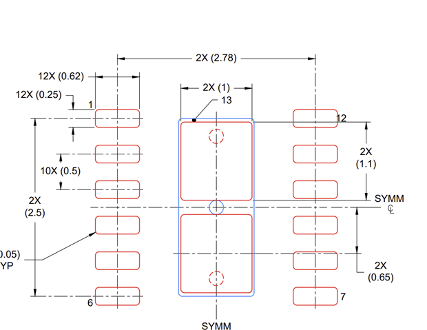
Could you please share the recommended land pattern for the part OPA547F/500?

We were unable to find this information in the datasheet. We’ve downloaded the relevant package from Ultra Librarian, but it provides three different decal options. Unfortunately, none of them match the mechanical dimensions specified in the datasheet.

To proceed with the PCB layout, could you please share the correct land pattern for this part?

Thanks in advance for your support.

  • Hey lathanivetha,

    No problem. I know we were bouncing between ALM2402 and the OPA547. I can provide you with the landing pattern for designing with the OPA547F/500. 

    Let me start by saying that some of these older parts have more options for landing pattern due to less uniformity across Burr Brown and TI. 

    I know that the Ultra librarian footprint will facilitate the OPA547, and honestly I may prefer that landing pad over what I have in my vault. 

    Here is my footprint for KTW7:

    The largest difference in my footprint vs. Ultra is the fact that my Y dimension on the thermal pad is a bit smaller relative to the top of the device pads. 

    It appears that my footprint also has taller pads relative to the Ultra model. 

    Both footprints will work perfectly fine. 

    If using V- connected to GND, I would certainly consider stitching the thermal pad to a GND pour to help with thermal dissipation. 

    Please let me know if you have any questions.

    Thanks,

    Jacob

  • Hi Jacob,

    Thanks for sharing the information.

    We will be connecting V- to the negative supply voltage. In this case, can the thermal pad  be connected to V-, or should it be handled separately?

    Additionally, could you please share the recommended land pattern for the ALM2402QDRRRQ1 IC?

    We've noticed a discrepancy between the WSON-12 package dimensions listed in the datasheet (3 × 3 mm, 0.5 mm pitch) and the decal provided in Ultra Librarian. The assembly value differs between both.

  • Understood here. 

    We can expect to connect the thermal pad to V-. In this case, it will be necessary to create a thermal pour on another layer of the board to help dissipate heat.

    Here is my footprint for the ALM2402 device: 


    Here is the footprint which should have been included in the DS:

    Both are valid implementations. Personally, I prefer the style used in my Altium, which should be the same as what Ultra has used. 

    What had a disparity in your eyes? the 3.1mm outside package dimensions can be understood as the max dimensions for the DRR package. 

    Thanks,

    Jacob