This thread has been locked.

If you have a related question, please click the "Ask a related question" button in the top right corner. The newly created question will be automatically linked to this question.

TLV9062: Different output behavior in Buffer and Differential Configuration

Part Number: TLV9062

Tool/software:

Hello TI Team,

I am using TLV9062 in two configurations. 

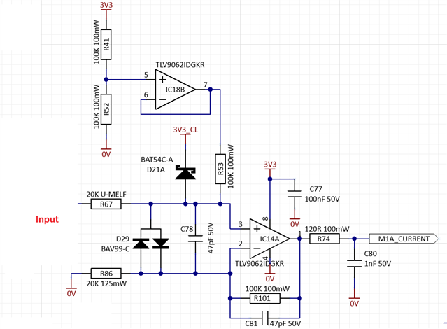
1) Buffer: Unity gain buffer with 1.65V offset

2) Diff Op-amp: Gain of 5 with 1.65V offset

Differential input voltage to circuit: 3mV to 400mV signal with 20KHz frequency.

This circuit amplifies voltage across MOSFET (Turn On state), in case of OFF state of MOSFET, input voltage increases upto 24V. Op-amp input terminal is clamped to 3.3V. So, every 50us op-amp output goes into saturation. As per datasheet it should come out of saturation mode within 200ns.

There is a different behavior of op-amp related output for two configurations.

In case of buffer, output settled within 2us and follows signal.

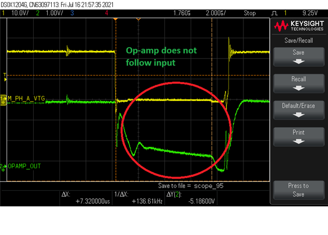
But in the case of amplifier (with gain 5) after settling time output does not follow input, it gradually reduces. Is it something related to slew rate of op-amp? Is there any relation between op-amp closed loop gain and slew rate? I have attached a waveform for your reference.
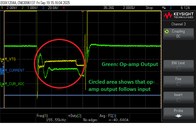
  • What is the yellow waveform?
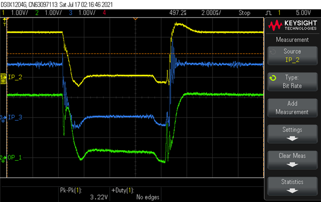
    Can you show traces of all three I/Os (pins 1, 2, 3)?

  • Hello

     Yellow trace is signal switched by MOSFET (0V to 24V). we are trying to measure voltage across MOSFET when mosfet is ON.

     I have captured the waveform at pin 1,2 & 3 of op-amp. Please have a look of attached waveforms.

  • Prasad,

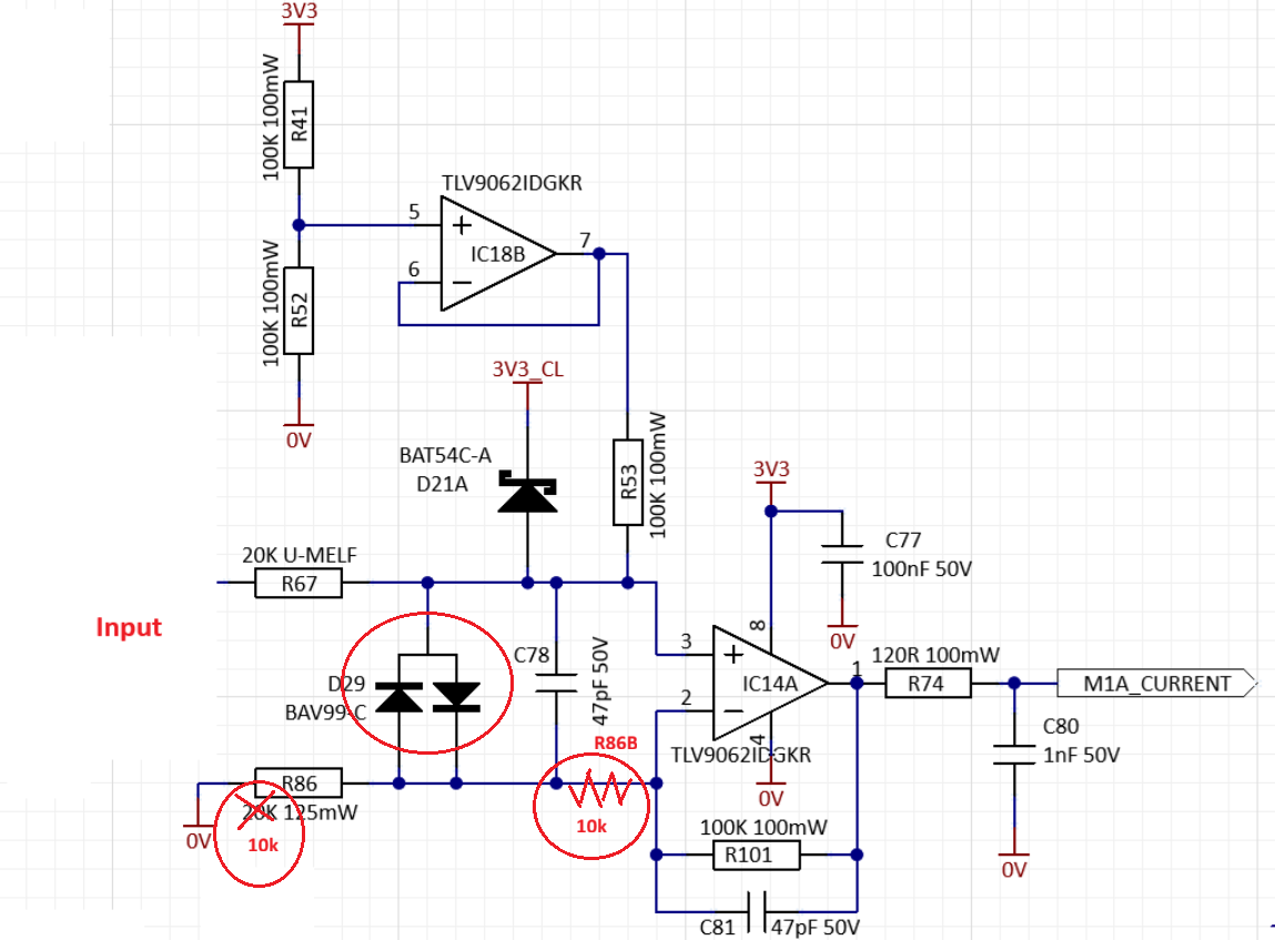
    I believe the issue is caused by the large junction capacitance of BAV99 diodes sitting directly on the inverting input of TLV9062.  The best solution may be to place 10k isolation resistor, R86B, by splitting R86 into two pieces as shown below (this will not affect the gain).

  • Hello Marek,

    Thanks for suggestion.

    I have run a simulation (Ltspice) with your suggestion, but I see some impact on the gain of the circuitry. I am about to modify circuitry for splitting R86 and rerun test on actual hardware.

    For understanding purpose, I have performed another experiment as below (Without splitting R86).

    • Isolated input from MOSFET and interface with signal generated.
    • Provided 0.1Vpp 20KHz input sine wave. I am getting proper amplified sine wave with gain with offset 1.65V at output.
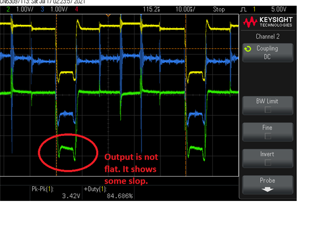
    • In 2nd iteration, instead of sine wave, I have provided square wave with 190mV & 50% duty cycle. I am getting amplified voltage at output. But I can see a significant increase in rise and fall time at output. I have attached a waveform. Please can you elaborate reason behind slow response at output?

  • I believe what you see is the effects of two 20k resistors and total input capacitance time constant of around 7us (see below).

    This would mean the junction capacitance of BAV99-C is around 62pF each:  TC=Rin*Cin where Cin = 2*Cj+C78+Cin_diff +Cin_Cm/2. 

    Cin = TC/Rin = 7e-6/40k = ~175pF.  Thus, Cj = [Cin-(C78+Cin_diff +Cin_Cm/2]/2) = [175pF-(47pF+2p+4pF/2)]/2 = 62pF

    Junction capacitance of each BAV99-C diodes is about 62pF.

  • Yes, it is related to delay introduced by capacitor.  I have removed capacitor C81, and it works perfectly. In the 2nd iteration C81 was placed and R86 & R67 changed to 1k1 and R101 & R53 changed to 5K1. It works fine.

    Thanks for support.

  • You should also eliminate C78 while C81 should be 1.2pF:    Rin*Cin = RF* CF, thus solving for CF=Rin*Cin/RF = 20k*6pF/100k