This thread has been locked.

If you have a related question, please click the "Ask a related question" button in the top right corner. The newly created question will be automatically linked to this question.

INA241A: INA241A: Current sense amplifier offset Issue

Part Number: INA241A

Tool/software:
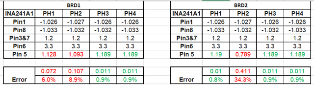
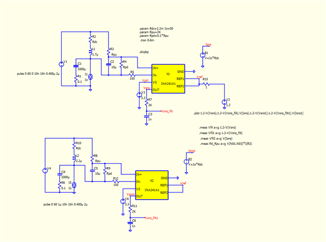
Currently using INA241A1 part to perform inductor DCR based current sensing for 48in/12Vo/250KHz 4PH interleaved GaN based buck converter application. 1.2V reference is supplied with external op-amp buffer. 

Seeing a big offset voltage issues at individual amplifier output and see similar performance too on multiple boards.  Initially everything looks good and over time the amplifier output voltage starts drifting with big offset. Circuit diagram and hardware reading for two different board attached.

Need help to understand the cause for this offset issue over time. Is this sometime to do with high dv/dt with GaN device or other issue? 

  • Hi,

    There shouldn’t be such a huge offset drift over time. To narrow down the scope, have you tried moving the devices around to see if the issue follows the suspect device? Or an A-B-A test?    

    Regards

    Guang

  • Yes swapping out amplifier is not working but replacing the bigger offset amplifiers with new one solves the problem for some times and again seen big offset over time.

    Do you see any issue with values of the external circuits components selected? Any concern with GaN dv/dt of 30V/ns ? Any alternate part suggestion? 

  • Hi Raju,

    Fast dv/dt shouldn’t be a problem, that is what this device is designed to handle.

    If the external component values are off, we should see accuracy issues from get-go. In my opinion, initially in spec but drifting out of spec over time is unlikely related to external components.

    The test data seems to suggest that there is no inductor current. Under this quiescent condition, the problem unit output is way off. Is my understanding correct? Have you analyzed if these devices are possibly damaged?

    Regards

    Guang

  • Yes just with bias supply turned on, we see offset issue at amplifier output. Analysis is not yet done, how to analysis for any possible damages on components as no physical damage observed ? 

  • Hi Raju,

    Can you elaborate on the test condition that the INA241 is configured in, with just Vs supply turned on? What about the inputs, are they connected to any defined voltage level, doesn’t matter it is 12V or GND. But they shouldn’t be left floating, otherwise you’ll observe the output issue similar to what you documented on some parts, sometimes.

    Regards

    Guang

  • Test condition is 48Vin/12Vo/250KHz/30A and the amplifier inputs are always connected across sensing capacitors as shown in above. Once the offset issue occurs during switching/powering up, then the output of amplifier have this offset with or without powering on. 

  • Hi Raju,

    Am I reading the table correct that pin 1 and 8 show about -1V to ground? Shouldn’t it be about 12V?

    Regards

    Guang

  • Hi Guang, The table is readings with auxiliary power only after the offset issue occurring during powering on. Yes the capacitor one end is electrically connected to Vo(+12V). Could you explain the cause of this big offset reading?

  • Hi Raju,

    It is still not clear to me how the input pins were measured -1V. If both INA input pins are connected to 12V, the offset should be within spec (ie small). Granted with some resistors, the offset will be slightly bigger.

    If you have a socket, you can verify the device offset directly. However the phenomenon you described doesn’t ring a bell assuming there is no issue with test setup. I don’t have an explanation for it, unless the device got damaged. An electrical test should be able to test if the device is damaged.  

    Regards

    Guang