Part Number: OPA657
Other Parts Discussed in Thread: OPA656
Tool/software:
Later I tried various methods, increasing the mask and reducing the noise to 1.5mVpp.
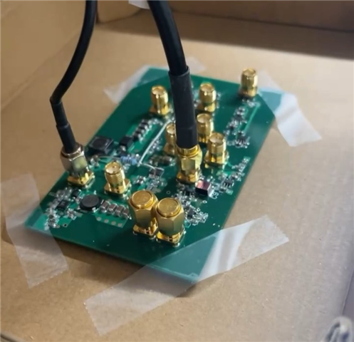
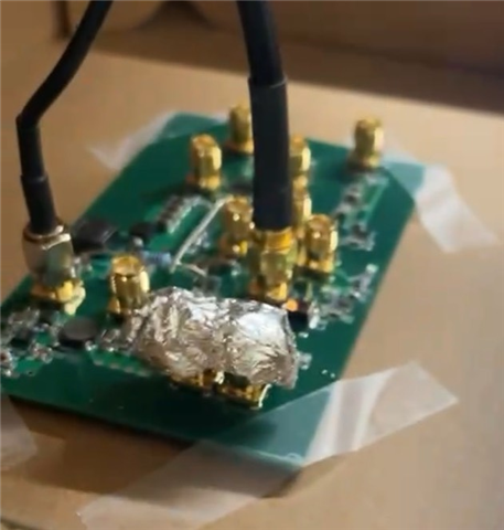
I've designed an interface circuit using an OPA657, but I'm experiencing some noise during actual measurements. The circuit has two inputs. I initially connected both inputs to ground using SMA shorting capacitors. I managed to detect approximately 30mVpp for a 60Hz signal. I assumed it was due to the room voltage, so I used aluminum foil as a shield, reducing the noise to 4mVpp.
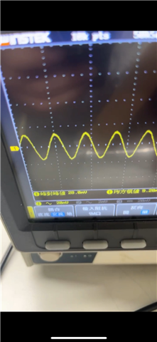
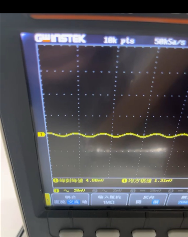
Later I tried various methods, increasing the mask and reducing the noise to 1.5mVpp.

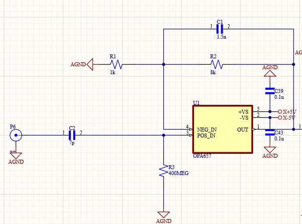
I'm interested in the noise behind my oscilloscope. Can I reduce the noise outside of the chamber? What's the best way to reduce it? Below is my schematic.


I would also like to ask about your knowledge of layout?