Tool/software:
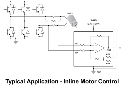
Hello, we use the INA241A-Q1 as an in-line shunt amplifiers for a 48V motor drive application.
When a motor phase goes high-to-low, or low-to-high, the common-mode voltage across the shunt change would cause a fair amount of noise on any amplifiers.
This INA241A blocks the vast majority of that noise, it's impressive.
My problem is that the drive is using fast-switching GaNFETs with a 100kHz frequency. Period is then 10us. When having a duty of less than 15%, the ADC sampling point is about 1.5us after transition, and that's where things go downhill:

Notice the INA241A lags a lot (1.5us) behind the phase current.
We suspected to be due to the PWM rejection mechanism, so we cooked up a little test: let the PWM toggle, and externally connect the load mid-period. This way, the common-mode voltage does not vary, but the current varies "instantaneously".

Now, the current probe is LAGGING 0.15us behind the INA241A!
This leaves me to believe the PWM rejection mechanism is mostly blanking based: When the common-mode voltage abruptly shift, it holds the previous value for ~1.6us.
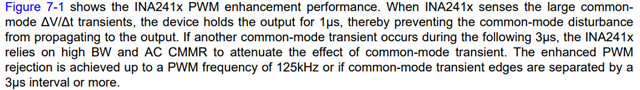
Of course, I'm suspecting I will be served with the good old "We can't tell you because our algorithms are proprietary trade secrets blablabla", [Edit, my bad, see Datasheet figure 7.1].
I'm mostly looking for advice on how to overcome the issue at hand.
Our patch for now, instead of sampling the phase current at mid-duty, we sample at mid-duty only when the duty is >50%, and at mid "off time" when duty < 50%.
Goal is to get away from the border conditions where the INA241A blanking interval will prevent operation below 15% duty.
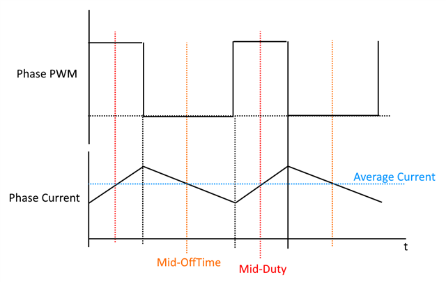
Due to the triangular and symmetrical nature of the phase current (when in continuous mode), both have the same value. It throws off some timing concerns as the ADC and PID/Controls timings are linked and they can widely jitter, with many phases adding to the effect.
The Questions!:
1- Is there any documentation about the effect we witness? Did I miss something in the datasheet or an app-note?
2- Is there any app-notes or guidelines on sampling point techniques to mitigate either that blanking or the PWM noise that is avoided?
Thanks!