This thread has been locked.

If you have a related question, please click the "Ask a related question" button in the top right corner. The newly created question will be automatically linked to this question.

OPA397: Buffer OpAmp choice for ADC inputs

Part Number: OPA397
Other Parts Discussed in Thread: OPA328, ADS131A04, TINA-TI

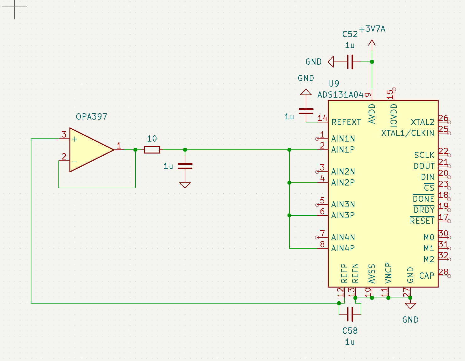
This is a follow-up for my previous question here: ADS131A04: Using REFP on analog input pins for TIA design - Data converters forum - Data converters - TI E2E support forums 

As suggested in the replies, I am looking to add a buffer to the REFP output of the ADS131A04 to ensure the current sourcing capabilities are sufficient. However, I am unsure how to choose the OpAmp exactly. Naively, I would expect e.g. the OPA397 to work, but it's unclear to me whether the bandwidth is sufficient to handle the rapid switching of the ADC sampling circuit? Would I need a faster OpAmp such as the OPA328, or something even faster?

For clarity, this is the circuit I am envisioning (the negative ADC inputs would be wired to the actual signal):

image.png

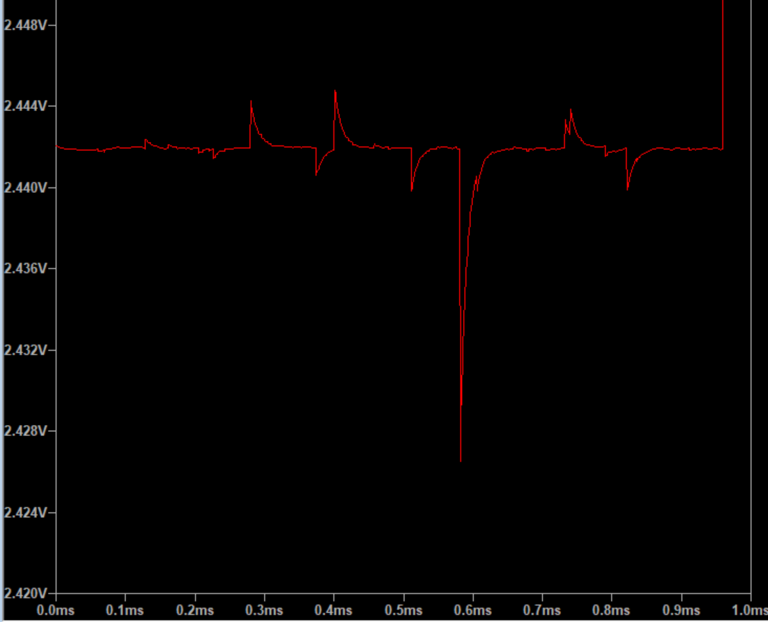
The lowpass after the buffer is there because I was worried about instabilities with the purely capacitive load from the ADC on the OpAmp (some rough LTSpice simulations seem to support this). I also tried to simulate the circuit to see whether the OpAmp is suitable, but I get some huge spikes from time to time, making me worried that something is wrong:

image.png

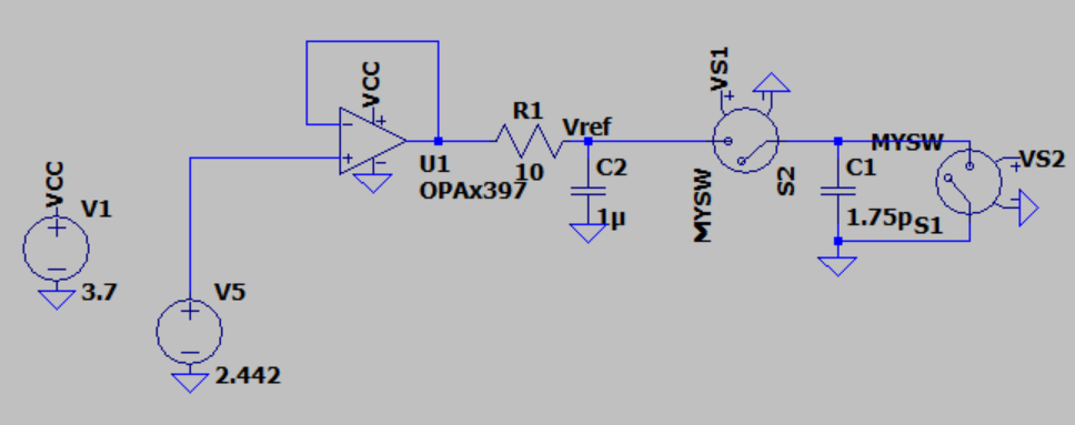
This is based on the circuit from Figure 38 from the ADS131A04 datasheet. The switches are set to 4MHz with an on-time of 0.12us, 180° out of phase.

What concerns me is that there are these random jumps away from the steady state (this is measuring the voltage at Vref, i.e. the input of the ADC):

image.png

So, in summary:

  • Is the OPA397 suited to buffer the ADCs REFP output for the ADC inputs? If not, what would be a better choice?
  • Do I need the lowpass filter after the buffer? Are the values reasonable?
  • In general, how can I verify that a given ADC is suitable, i.e. how do I model the ADC circuitry, and what do I need to look for?
  • You do not specify sampling frequency, required settling time and resolution BUT your RC with time constant of 10us (10ohm*1uF) would result in a very long settling tail - see below.

    Thus, I believe you need to use a faster op amp like OPA328 with much lower ESR resistor - please review white paper by clicking the link below:

    https://www.ti.com/lit/an/sboa558/sboa558.pdf?ts=1760983421469&ref_url=https%253A%252F%252Fwww.ti.com%252Fproduct%252FOPA328

    Using OPA328 with ESR of 360mohm (or greater) results in 45 degrees minimum recommended phase margin (or higher) - see below.

    Running transient analysis shows stable operation with much faster settling time - see below.

    I have attached below Tina-TI simulation schematics.  you may download a free version of Tina-TI by clicking on following link: https://www.ti.com/tool/TINA-TI

    OPA328 AC Stability.TSC

    OPA328 Transient Stability.TSC

  • Thank you for the detailed response! I will try to go through your suggestions in more detail. In the meantime:

    • The target data rate is 10-20kS/s, with the modulation frequency set to 4MHz. The question regarding settling time is not fully clear to me, as the OpAmp is only used for the "steady state" reference input?
    • Could you explain the logic behind the first simulation that you show? What exactly are you probing by "disturbing" the circuit at the OpAmp output? Why is the settling time to disturbances there relevant for the functioning of the circuit? Naively, I would have expected that I need to "disturb" the circuit after the low-pass & check that I get the "correct" voltage stored in the sampling capacitor (i.e. that the sampling capacitor can be charged properly & that the impedance is not too high). Since the average impedance is >100kOhm, I assumed that the 10Ohm resistor combined with the comparatively large 1uF capacitor would provide enough DC current & enough transient response (since the 1uF capacitor can charge the sampling capacitor ~500'000 times, or ~125ms, i.e. way longer than the time constant of the lowpass filter). Your comment suggests to me however that I am missing something here?
  • The reference input voltage is in a steady-stead BUT Vref gets disturbed by sample & hold during each sampling cycle due to switching S2 and charging C1 - see below.  Thus, it takes time for the Vref to settle before conversion inside ADC may take place. That's another reason why I reconfigured location of ESR.  

    In order to optimize the RC filter in fron of ADC, please download TI Analog engineer calculator by clicking on following link:

    www.ti.com/.../ANALOG-ENGINEER-CALC

    You may determine stability of the circuit by stimulating output with a small-signal (<10mV) and making sure that the overshoot is less than 25% - this corresponds to recommended minimum 45 degrees phase margin. In the case of a buffer, you could accomplish this by either applying a square input voltage or by exciting the output with current pulses but in some other circuits with feedback capacitors (which filter out the square signal) you have to directly stimulate the output with square current pulses.  In the case of OPA328 the overshoot is 24%, thus meeting the maximum recommended value of 25% - see below.

    However, in the case of OPA397 the overshoot is 56%, which may be estimated to have ONLY 20 degrees (instead of 45 deg ) phase margin - see below.  This is way too low phase margin to assure stability over wafer process and temperature variations.

    Please review TI Precsion Labs stability tutorial under following link: https://www.ti.com/video/series/precision-labs/ti-precision-labs-op-amps.html