


Part Number: OPA615
Using the OPA615 as an SOTA as shown below:
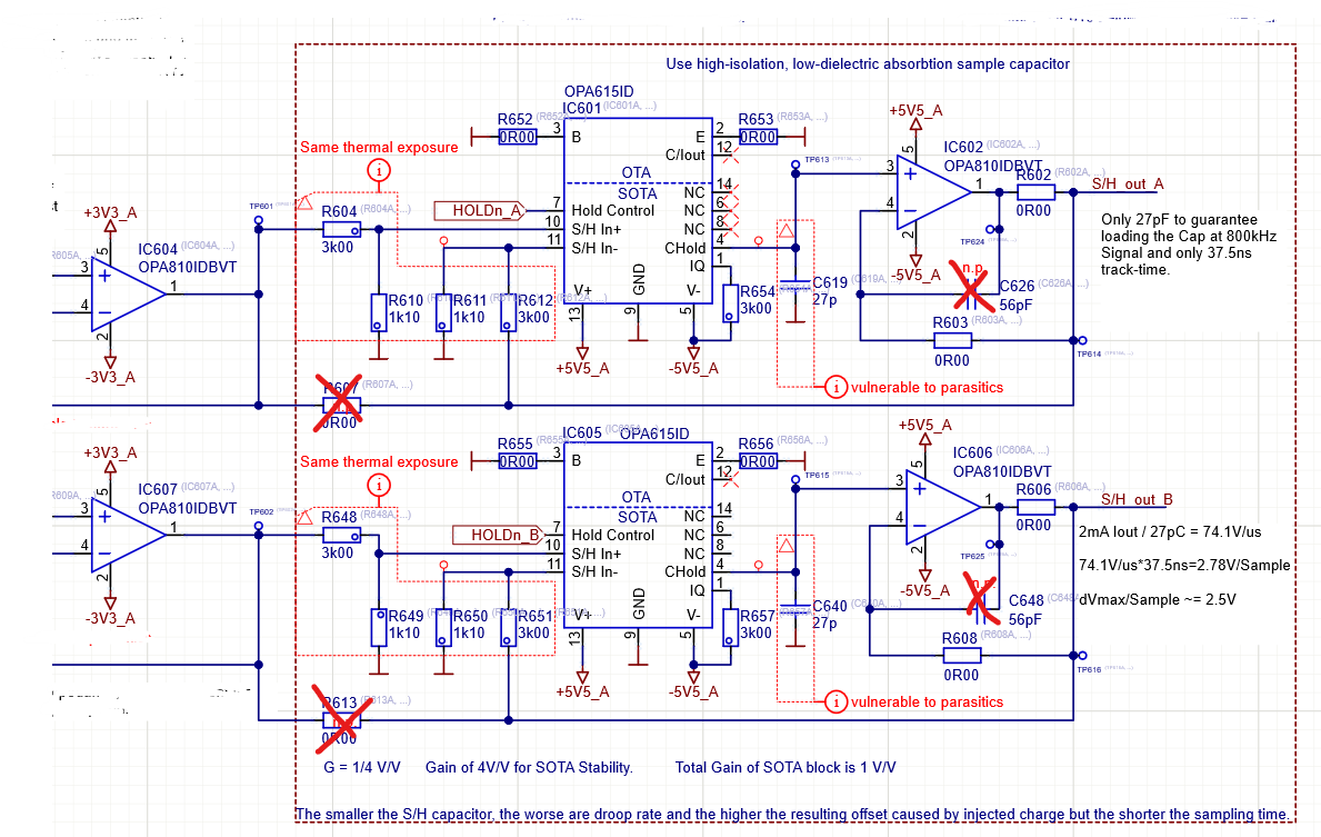
The stability of the circuit seem to be fine and behaves as simulated. I know that the Hold Capacitor is small but this is necessary for the required track time. Increasing the Hold Capacitor will ease my in the folllowing presented problem but is not really an option.
Problem is what seems to be the switch inducted charge when switching to hold mode. In the picture below, the yellow signal (CH1) is showing the S/H_out with an additional gain of 5.33 and the blue singal (CH3) is the HOLDn signal with 200ns period and 40ns duty. For this measurement the OP615 is sampling GND-potential.

The problem is not the induced Offset but its variation in time that appears as "low-frequency" noise. As the measurement shows, the minima of the S/H_out signal during HOLDn "high" is representing the "true" Signal. But the induced offset that appears after HOLDn goes "low" is not a constant but changing.
So I need to know if this is expected behavior of the device or is there potential to improve?
The HOLDn Signal is appearing well enouth on the scope, it is perfectly separated by GND-Plane in the layout from analog parts. I do not think that the effect is dielectric absorbtion of the Hold-Capacitor, since the absorbtion would be in the same range as the original charge. I also experimented with different quiesent currents Iq ranging from 8 to 13mA. Tryed different Logic Levels for HOLDn. The OPA615 decoulpling capacitors 4u7F, 100nF and 1nF at each rail to GND.
Is the OTA-Part fine with bounded to GND at B and E or will it oscillate or drawn extra power? Could the "high" resistance at In- at the SOTA Input be a problem? Are NC pins fine with floating?
I felt in exitement working with this device and hoping to get this last remaining problem solved.
Best regards,
Tom
