


Other Parts Discussed in Thread: SN74AUC74
Hello everyone,
I am currently trying to develop a circuit that uses a TLV3801. To simulate the components I am using LTSpice. The basic idea is to feed the non-inverting input of the TLV3801 with a high frequency (216 MHz), low amplitude (200mV) sine wave so that a 216 MHz square wave gets generated on the output.
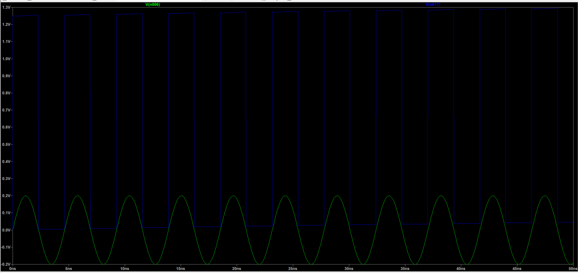
So far the accomplished results look very promising. I've added a few screenshots to show you the obtained signals:

The green signal is the 216 MHz sine wave and the blue signal is the out+ pin of the TLV3801. So far so good. Now the problem is that in the next stage I need to feed that square wave into a d type flipflop (SN74AUC74) which operates at around 1.8 V VCC. Hence the flipflop's high-level input voltage is roughly 1.2 V which fits perfectly. But the low-level input voltage is about 0.6 V according to their data sheet. So the above square wave could not be used like this because it would actually never turn off the SN74AUC74.
So I was experimenting a little bit and somehow got the perfectly shaped square signal for my specific application by slightly modifying the above circuit. See the screenshots below: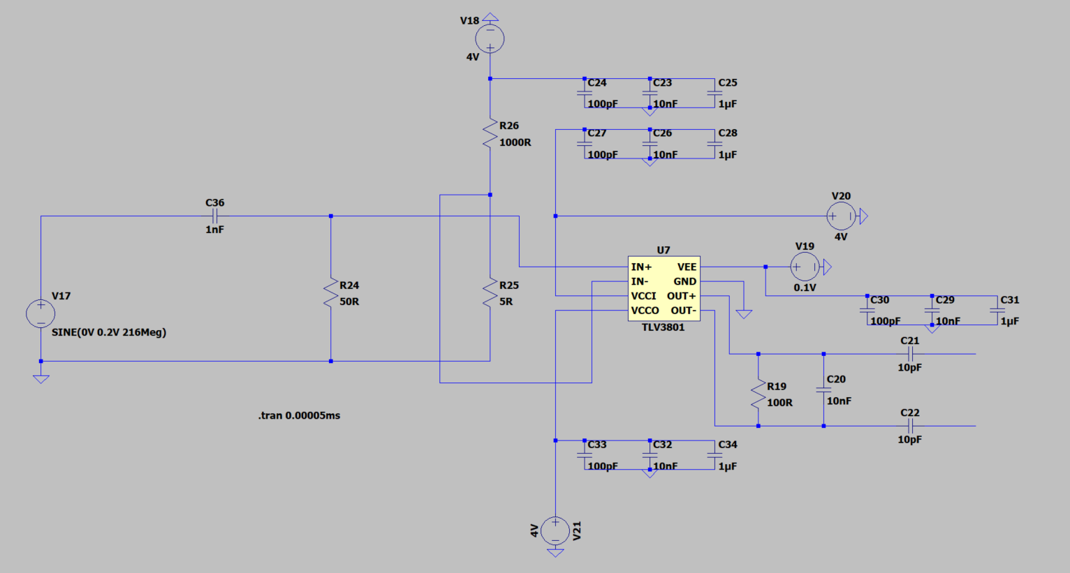
Now comes the actual question - Can the VEE value of a TLV3801 be slightly higher than GND? When I put VEE around +100 mV the circuit seems to work pefectly fine (see the above blue signal). There is a little drift causing the lower value on the out+ pin to slowly increase from 0 V up to a maximum of about 120 mV but still that signal would be perfectly fine for my use case. If I set VEE to -100 mV, -50 mV or even +50mV or +200 mV there is no signal on the out+ pin. So +100 mV seems to be the sweet spot. Is this just a numerical issue / not a realistic result? Or would it actually be technically possible to set VEE to 100 mV even though if it is expressly not recommended because it exceeds the maximum ratings of the IC?
If I'd try to pull down the lower threshold of the TLV3801 LVDS output using another comparator I'd probably fight with additional propagation delay and also wouldn't see such wonderfully clean and sharp square like edges like those of the blue signals above. So I wanted to try to avoid using a lot of additional circuitry. Maybe you guys have some advice for that issue.
Thanks a lot for your time and interest,
Laule


