This thread has been locked.

If you have a related question, please click the "Ask a related question" button in the top right corner. The newly created question will be automatically linked to this question.

OPA355: Non inverting amplfiier designing

Part Number: OPA355
Other Parts Discussed in Thread: TINA-TI, OPA838, THS4551

I am planning to design front end for ADC .. with low noise

if fC of filter is 10MHz and Input signal frequency is 500KHz then 

So intial stage is Non inverting amplifier - so

  1. To eliminate error due to offset shall i use Capacitor at input ? and can u recommend any document to select that capacitor..
  2. If my gain is 10 then should i chose GBW of atleast 10*500KHz or 10*10MHz ?
  3. To eliminate noise i want to keep capacitor in feed back or want to use RC at output of Non inverting op amp & Shall i limit op amp BW to 500KHz or 10MHz ?
  4. I want to use 4th order filter , will filter eliminate noise due to Non inverting amplifier? & will filter also generate noise ? if generates , cascaded nxt stage can eliminate the previous noise?
  5. Please suggest op amp for my requirements for Non inverting amplifier and Filter designing.
  • Hello Sruthi,

    1. The capacitor at input is useful to block DC signal, this will eliminate DC error from your input source/stage. If DC information is not needed, this can be selected as your high-pass filter depending on your resistor at your input and of course below your input signal frequency of 500kHz. We usually use 1uF to 100uF capacitor to have a low cut-off frequency. If you are using a single-supply design which is usually the case to drive ADCs, then these app notes will be very useful to guide you on AC-coupled design then adding a DC signal for shifting your common mode to meet the amplifier's input/output voltage range and your ADC's specification.

           https://www.ti.com/lit/ug/tidu871/tidu871.pdf?  and https://www.ti.com/lit/an/sboa224a/sboa224a.pdf? 

      The amplifier does contribute internal error (DC offset voltage and bias current), this will be reflected to the output. If you want to reduce offset error as well, you can add the AC coupling capacitor at the output of the amplifier as well, and this will be the same value. When using single-supply configuration, you would need to re-add the DC reference voltage again after the AC coupling capacitor to your ADC. 

    2. Yes, you are correct. The estimated GBW you would need would be 10*10MHz at your frequency cutoff. Since your input signal frequency is 500kHz, you could lower your frequency cutoff if needed. 

    3. Yes, exactly, you could do an active low pass filter followed by a passive 2nd order filter to limit BW to closer to 500kHz.

    4. Having a 4th order filter would help with having a steeper roll-off at your frequency cutoff. You are correct that the extra components can generate additional noise, but depending on the values chosen and temperature of application range, it could be not dominant noise factor. We could tune/try these possibilities in a simulator, either Tina-TI or PSpice. 

    5. We can help suggest and design the amplifier + filter to your ADC. Have you chosen your ADC? If not, do you need single-ended or differential input? What is your supply voltage requirements? 

    Thank you,

    Sima 

  • Thanks for the reply, Sima.

    I have one follow-up question regarding the analog front-end design.

    Our input signal is in the order of a few microvolts, generated by a photodiode. To increase the signal amplitude, would you recommend using an inverting amplifier or a non-inverting amplifier? Please share your reasoning considering noise performance and stability.

    At this stage, we have not finalized the ADC selection. The input signal is mostly single-ended, but I would appreciate suggestions for both single-ended and differential approaches.

    Design constraints and requirements are as follows:

    • Input signal frequency: 500 kHz

    • Required gain: 11

    • Application: Low-noise analog front end

    • Anti-aliasing filter cutoff frequency: 10 MHz

    • Filter gain: 1

    • ADC supply voltage: 3 V

    Based on the above, could you please suggest:

    1. A suitable op-amp for the amplifier stage (low-noise requirement)

    2. A suitable op-amp for the filter stage

    3. Key design considerations and precautions to take while designing this analog front end (noise, bandwidth, stability, layout, etc.)

    Looking forward to your guidance.

  • Hello Sruthi,

       For the photodiode, these are most of the time a current output unless it is with an IC with either a TIA (transimpedance amplifier) or resistor to produce a voltage output. I wanted to confirm if the previous statement is true where it is integrated and will be a voltage output, or you will need a TIA stage for the current-to-voltage conversion. 

      If a TIA stage is needed, then this would be your first low-noise stage, then we would follow this up with a passive 2nd-order filter to a single-ended ADC or a active 2nd order fully differential amplifier filter + passive 2nd order filter then a differential-ended ADC. And, in that case, the required gain would be focused on the first TIA stage which will give the lowest overall system noise.

      Let us know which statement is correct above, and we can help guide the design for single-ended and differential case with emphasis on low noise. If TIA stage is needed, then also please provide the internal capacitance of the photodiode at the reverse bias you will use. 

    Thank you,

    Sima 

  • Hi Sima,

    Our input source is a photodiode module with an inbuilt TIA, so the output is a voltage signal. Based on initial assumptions, the output voltage level is expected to be in the uV-millivolt range.

    We are planning to use a non-inverting amplifier to scale this signal to the volt range. After amplification, we intend to implement a 6th-order Bessel low-pass filter before feeding the signal into the ADC.

    At this stage, we are not fully clear on whether the signal chain should be implemented as single-ended or differential, and we would appreciate your guidance on this aspect.

    Please let us know your thoughts or recommendations based on similar applications.

    Best regards,
    Sruthi

  • Hello Sruthi,

      Thank you for the confirmation. 

      There are couple pros/cons to using single-ended vs differential ADC. For a differential signal, this is useful if you are planning running longer cables/traces and the differential set-up will help cancel out the noisy environment. Differential signaling also maximizes dynamic range, improves distortion by cancelling out even-order harmonics, and still helps with noise. While the advantages of single-ended signaling are: lower cost, decreased size, and less components. 

      Here is an example with our suggested device of OPA838 for single-ended design:

      Design uses your requirements of 3V single supply, 11V/V gain, 6th order Bessel Filter. I am using 1mV source, you can adjust gain + filter for your input source if your source is closer to uV range. And, you can adjust filter cutoff for closer to 500-600kHz for lower noise, and the common-mode voltage output to match ADC's required common-mode voltage via V1. 

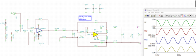
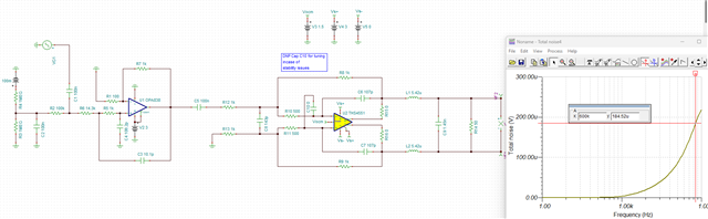
      And, here is an example with our suggested devices of OPA838 and THS4551 for differential-ended design:

      Design uses your requirements of 3V single supply, 11V/V gain, 6th order Bessel Filter. I am using 1mV source, you can adjust gain + filter for your input source if your source is closer to uV range. And, you can adjust filter cutoff for closer to 500-600kHz for lower noise, and the common-mode voltage output to match ADC's required common-mode voltage via VOCM pin. 

    OPA838 Bessel Filter.TSC

    OPA838_THS4551_BesselFIlter.TSC

    Thank you,
    Sima