


Part Number: LM293
Hi Team,
This concerns a TI LM293DR comparator used in a Solar OCP (Over-Current Protection) application. We have discovered the following issue during testing and request your assistance:
Problem Description:
Customer's designed circuit (see attached plot below) shows that under normal temperature conditions, when Pin 5 voltage is higher than Pin 6 voltage, the output L_OFFINV_S is High. However, when the ambient temperature reaches 60°C, even though Pin 5 voltage remains higher than Pin 6 voltage, the output unexpectedly transitions to Low. Why does the output change to Low at 60°C when Pin 5 is still higher than Pin 6, especially since this temperature is within the operating range and the output should remain High?
Are there any adjustments needed in the circuit design?
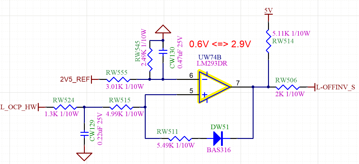

Additional Information:
The L_OFFINV_S signal subsequently connects to 12 AND gates, with 12 identical groups as shown in the second circuit diagram.
Test Results:
At 25°C (see Plot with 25Degree):
Pin 5 voltage > Pin 6 voltage
L_OFFINV_S output: High level
Status: Normal operation

At 60°C (see plot here):
Pin 5 voltage > Pin 6 voltage (still higher)
L_OFFINV_S output: Low level (unexpected)
Status: Abnormal behavior

Expected behavior: L_OFFINV_S should remain High when Pin 5 > Pin 6, regardless of temperature within the operating range.
Actual behavior: L_OFFINV_S transitions to Low at 60°C despite Pin 5 still being higher than Pin 6.
Please advise on the root cause and potential circuit modifications.
Regards
Brian

