This thread has been locked.

If you have a related question, please click the "Ask a related question" button in the top right corner. The newly created question will be automatically linked to this question.

INA293: The schematic diagram review for INA293A2IDBVR

Part Number: INA293

Hi,

We use the INA293A2IDBVR for the current amplifier, and now, INA293A2IDBVR is a chip placed on the power bus for current sampling, with a voltage tolerance range of -4~110V, our input voltage is 48VDC, Is this voltage tolerance range related to whether the chip is powered or not? If the chip is not powered and there is a voltage of 80V between VIN+ and VIN-, will it cause damage to the chip?

Our schematic diagram please refer to below:

6991db88ca84163b05eddd7878afdb04.jpg


  • Hello Zhang,

    , Is this voltage tolerance range related to whether the chip is powered or not?

    It is irrelevant if the part is powered on but GND is the reference to everything if GND is floating there could be issues as all absolute max voltages are rated to GND.  Also some devices can latch up if the input pins have a transient while the VS pins are floating.  If connected to 0V there is no risk.

    If the chip is not powered and there is a voltage of 80V between VIN+ and VIN-, will it cause damage to the chip?

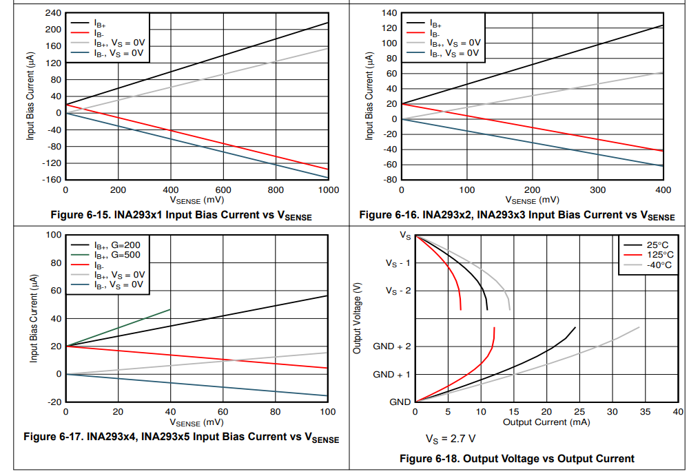
    It will not cause damage we even have a plot of IB with Vs = 0V.