This thread has been locked.

If you have a related question, please click the "Ask a related question" button in the top right corner. The newly created question will be automatically linked to this question.

INA851: Large DC offset removal

Part Number: INA851
Other Parts Discussed in Thread: TINA-TI, THS4536

Hello,

I'm trying to remove a large differential DC offset in my design including INA851 FDA.

I'm familiar with DC servo loop circuit and I also know that In-Amps such as AD8220 have a REF pin to be used within an integrator circuit in order to compensate the DC offset, and remove the DC offset and AC-couple the signal.

my question is how to remove the DC offset in FDA circuits? Is the Vocm of INA851 as an FDA similar to REF pin in In-Amps like AD8220?

Best,

Hadi

  • Hi Hadi,

    Thanks for using E2E! I have not seen a DC offset removal circuit for a FDA, but I can help find you a potential solution. Do you know what the input waveforms are in your system (amplitude, offset, frequency) as well as what the output is connected to (another amp, ADC, etc.)?

    The Vocm pin sets the reference for both outputs, where VOUTP = G(Vin+ - Vin-)/2 + Vocm and VOUTN = -G(Vin+ - Vin-)/2 + Vocm.

    I am not sure if this is possible without using high pass filters at each output. Can you let me know what offset you are trying to remove? Is it the common-mode offset created by Vocm, or do you want to remove any differential offset at the output? 

    Best Regards,

    Taylor Allan

  • Hi Taylor,

    Thank you very much for your prompt reply.

    Indeed I have a differential input ADC at the other end, and therefore, I need to remove any differential DC offset up to 300mv.

    The gain is high, 400v/v. One weak and easy solution is to reduce the gain to avoid clipping and then remove the DC after the ADC.

    I know I must solve it with a high-pass, but the question is where should I apply the compensation to? 

    Is it the FDA_IN+/-, Vocm, or even RG pins?

    I also found a couple of helpful content like this: https://upcommons.upc.edu/server/api/core/bitstreams/85723f74-872b-43f3-8022-faca49781cd3/content. However, I can't implement the HPF circuits as done in this article, in the INA851.

    Kind regards,

    Hadi

  • Hi Hadi,

    You would not be able to use the Vocm pin, as it would only be able to eliminate common mode offset, which wouldn't solve your problem.

    For the 300mV offset, is this based on a DC differential that you expect on the input? The INA851 shouldn't have an offset greater than ~30mV worst case with a gain of 400. 

    After looking over this, I think the only way to eliminate any offset would be to have a bandpass filter on the output (if you are also designing a LPF for the ADC input), which targets the frequency of the input signal. Something like this below:

    If you would like, I can help with finding the right component values for your filter. Do you know the frequency you are targeting?

    I do have some ideas of how you could possibly achieve this with a servo loop and have been testing them in simulation, but I will likely have to test it in lab to verify. I will make sure to respond if I find a solution in lab.

    Best Regards,

    Taylor Allan

  • Hi Taylor,

    Thanks for the HPF solution.

    I try my best to avoid placing any passive RC components on the AFE so as not to compromise CMRR, though.

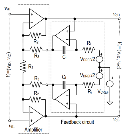
    The image above shows one way to remove DC offset. However, I couldn't figure out which pins the integrators should be connected to on the INA851.

    I know it's different from the internal circuitry of the INA851, but it can be used as an idea.

    The REF pin of input amplifiers like the AD8220 is used to feed the integrator to them and remove DC, and everything you find on the internet about DC removal is actually about the REF pin and the same method. I wonder why no one has discussed DC removal for the FDAs.

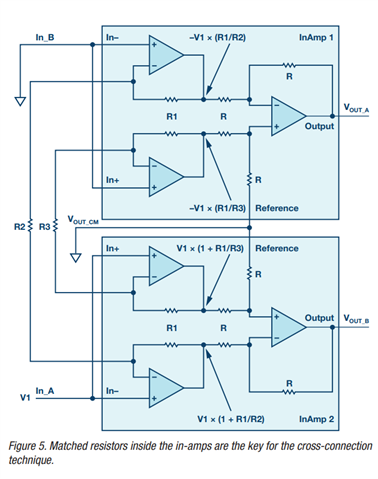
    By the way, since simulating the INA851 in LTspice takes a long time (using the INA851 Pspice file from the TI page), I tried to find a simpler equivalent circuit with ideal op-amps. I found that you can use two In-Amps like the one in the picture below to make an FDA.

    As a side result, I found out that the VOCM is made of connecting both In-Amps' REF pins, and that ensured me that the Vocm can't be used for DC offset compensation.

    Please share your ideas on DC servo circuits, I can simulate and test them in my lab. I'm curious to see where the DC servo loop is connected to.

    Best regards,

    Hadi

  • Hi Hadi,

    Thanks for the input! I see, I understand why you wish to use a servo loop then. I have come up with a possible solution that currently works in simulation below. 


    Essentially, injecting equal but opposite currents into the RG pins will allow for internal compensation for the differential offset. The tradeoff comes with choosing the values of Rinj, as smaller values can effect your differential offset, while larger values can cause the output of the integrator amp to saturate. I added an input offset that corresponds to a 300mV DC differential offset without offset removal, and get a 0.94mV DC differential offset on the output using the servo loop with 1% tolerance injection resistors.

    As a side note, the INA851 SPICE model shouldn't take a long time to run on either PSPICE or TINA-TI, if you wish to use either of those. I have personally been using TINA-TI for these simulations. I would also recommend selecting/adding 1G of parasitic resistance for the 100n capacitors so that the simulation can find a DC operating point.

    Best Regards,

    Taylor Allan

  • Hi Taylor,

    This circuit works. However, I meant that 300mV DC offset appears at the inputs (so, +/-300mV), which means that adding 375µV offset to the input in the simulation is not enough. Even values ​​less than 300mV, say 100mV DC offset, will saturate the amplifier, which I think could be adjusted by reducing Rinj to inject much more current for compensation, but I think reducing it would affect the offset, and I think the gain, as you mentioned.

    I designed a similar integrator circuit, but I applied it to the FDA_IN pin of the INA851 to inject current for compensation, which was not a good idea.

    However, I have a few questions about your design:

    Is it intentional to have different resistor values ​​of 80.8kOhm and 79.2kOhm for Rintj+/-?

    Does this approach affect the gain accuracy, especially if Rintj is reduced to inject more current?

    I still suspect that FDAs are not meant to be used in situations where there is a large DC offset and In-Amps are still the best choice due to the REF pin being dedicated by an integrator feedback to compensate for offset.

    However, my ADC is a differential input, and I can't use a single-ended amp.

    Best,

    Hadi

  • Hi Hadi,

    This circuit works. However, I meant that 300mV DC offset appears at the inputs (so, +/-300mV), which means that adding 375µV offset to the input in the simulation is not enough. Even values ​​less than 300mV, say 100mV DC offset, will saturate the amplifier, which I think could be adjusted by reducing Rinj to inject much more current for compensation, but I think reducing it would affect the offset, and I think the gain, as you mentioned

    Sorry, I assumed that you meant the 300mV offset was at the output.

    You are correct, by injecting more current to compensate for a larger offset, the gain error increases. Below shows how the GE increases as the injection resistor values are reduced for a 1V amplitude output waveform. For the 300mV input offset, I had to use injection resistors in the hundreds of ohms.

    Is it intentional to have different resistor values ​​of 80.8kOhm and 79.2kOhm for Rintj+/-?

    I intentionally added 1% tolerance to the injection resistors to see the effect on the output. The tolerance in this case does not seem to be crucial, as the resistor values are chosen so that the needed injection current doesn't causes the integrator to saturate. Using the simulation, I was able to confirm this as the remaining output offset was independent of an increase in resistor mismatch.

    I still suspect that FDAs are not meant to be used in situations where there is a large DC offset and In-Amps are still the best choice due to the REF pin being dedicated by an integrator feedback to compensate for offset.

    I believe that in this case that is true depending on the allowable gain error of your system, as the input offset is so high for the given gain that low resistor values are required.

    I don't believe that you would be able to achieve the offset removal with a single-ended INA with a conventional servo loop, as the internal nodes of the device become saturated and adding in a correction via the reference will no longer help. This is based on what I have tried in the simulation tool, but I will put together a simulation of the internal structure to verify and respond with my results. If this isn't the case, you could use a single-ended to differential circuit with the THS4536.

    Best Regards,

    Taylor Allan

  • Hi Taylor,

    This circuit works fine in LTspice too. However, I see more gain error than yours.

    I simulate with zero conditions to see the effect of capacitor charging/discharging. That may be why I see this gain difference.

    According to my measurements, at least about 14.5 mA should be injected into Rinj, otherwise FDA will saturate.

    Wouldn't it be better to add a resistor in parallel with the integrator's feedback capacitors to prevent saturation?

    In general, are there other ways to remove DC offset faster than with integrator feedback? I understand that this is an inherent behavior of the integrator and is a trade-off between bandwidth, aggressiveness and frequency response.

    One solution that came to mind is to use a different path for higher DC offset voltages, for example using a series diode with lower resistance. However, this affects the integrator cutoff freq, but on the other hand, it accelerates DC nulling or settling time.

    Best regards,

    Hadi

  • Hi Hadi,

    I simulate with zero conditions to see the effect of capacitor charging/discharging. That may be why I see this gain difference.

    What is the gain error that you are seeing in this case? I am curious as to how large this difference is.

    According to my measurements, at least about 14.5 mA should be injected into Rinj, otherwise FDA will saturate.

    From my understanding, the injection current will vary depending on the differential offset on the input, and the resistor value will determine whether the FDA saturates (voltage at the output). For example, the injection current for using a 100Ω injection resistor is the same as using a 300Ω injection resistor (20.05mA). So if you are using a 350Ω injection resistor, the maximum injection current should be ~14.3mA (corresponding to ~214mV of input offset) for a +/-5V supply.

    Wouldn't it be better to add a resistor in parallel with the integrator's feedback capacitors to prevent saturation?

    Yes, this should work to extend the range of injection resistor values possible without saturating the FDA (by decreasing the injection current). However, the tradeoff here is that an increased DC offset is introduced on the output, and this offset will increase as you decrease the feedback resistor. 

    In general, are there other ways to remove DC offset faster than with integrator feedback? I understand that this is an inherent behavior of the integrator and is a trade-off between bandwidth, aggressiveness and frequency response.

    The only other way that I am aware of is to use a passive HPF on the input or output which as you said introduces CMRR issues. Another possible solution would be to have a DC offset removal stage, with the INA851 in a gain of 1, before a separate gain stage. The issue with this of course is that generally you want the gain stage to be the first stage in your signal chain, as the previous stages' noise/offset/etc. gets amplified. However, this might be necessary in this system.

    One solution that came to mind is to use a different path for higher DC offset voltages, for example using a series diode with lower resistance. However, this affects the integrator cutoff freq, but on the other hand, it accelerates DC nulling or settling time.

    The only potential issue that I see is with introducing nonlinear components, where you are likely introducing some distortion/temp drift/etc., plus any stability analysis becomes difficult. Are you able to test this in lab? Because I have not seen this circuit operate before, I am wondering how well this overall circuit performs outside of simulation. If not, I can test it myself to see how well it operates.

    Best Regards,

    Taylor Allan