This thread has been locked.

If you have a related question, please click the "Ask a related question" button in the top right corner. The newly created question will be automatically linked to this question.

TLV9154: Burn-test problem check

Part Number: TLV9154
Other Parts Discussed in Thread: TLV9152

Hi team,

The customer encountered an issue during the burn-in test.
Test conditions:
Ambient temperature: 45°C
Input: 300 Vac / 50 Hz
Output: 48 V / 90 A
After approximately 30 minutes of burn-in, high-frequency noise was observed on the OPA output. This noise interferes with the control loop and causes a momentary increase in output power, which then triggers OCP protection.
The issue typically occurs after nearly 30 minutes of burn-in, at which point the IC temperature may rise above 90°C. We have also confirmed that the IC Vcc voltage remains stable at 3.3 V during the event.
From the waveform, it appears that a sudden rise in the OPA output may be causing the control malfunction. Since this phenomenon only occurs at high temperature, we suspect that the OPA may be entering thermal protection due to overheating.
We would like to ask:
1. What could possibly cause this type of waveform behavior?
2. For this condition, are there any recommended thermal improvement solutions? (ex: are there any internal thermal pin for this device?)

Waveform channels:
Ch1: DAC (represents Vout feedback = OPA output)
Ch2: Iout
Ch3: Vout
Ch4: Iout feedback (OPA output)
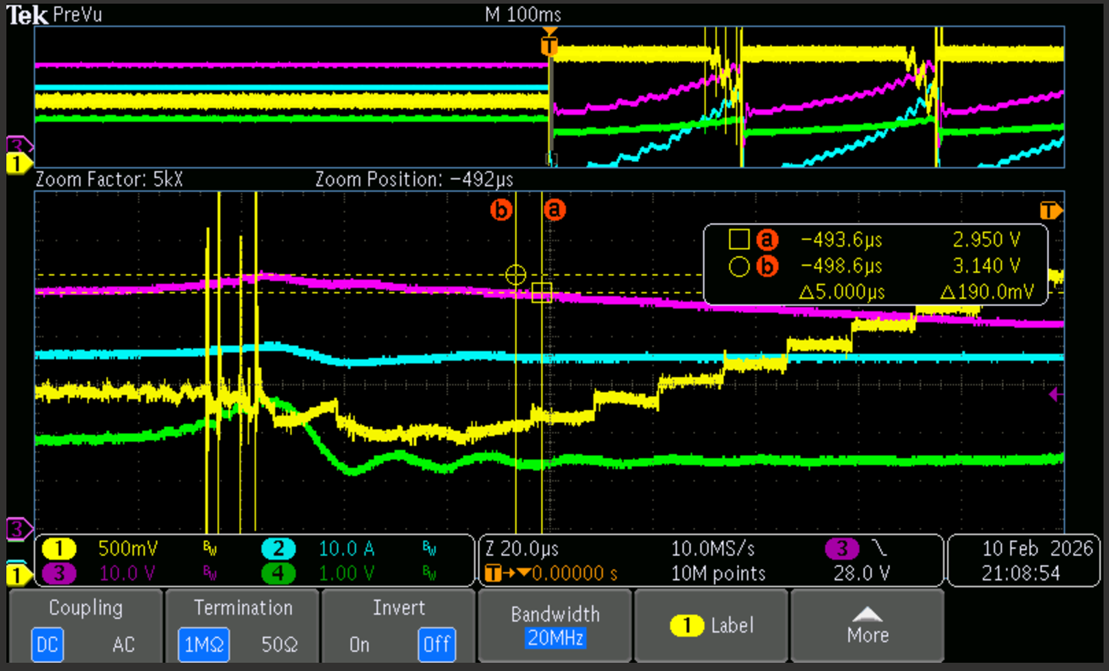
image.png


Thank you.

  • Hi Jenny, 

    It is difficult to determine the root cause with the information provided. Based on the burn-in conditions described, one possibility is that the device's thermal protection may be activating, particularly if there are significant output current demands on the TLV9154. 

    Are you able to share additional information such as:

    • Schematic
    • What is the output current that is being demanded from the TLV9154
    • What is the supply condition of the TLV9154
    • Any other relevant details would be appreciated. 

    Note that the device has thermal protection and if it is indeed kicking in, you may see unexpected behavior. When thermal protection engages, the output stage can momentarily disable. This loss of drive may appear as unexpected transitions in a control loop system. See the excerpt from the datasheet below.  

    Best Regards, 

    Chris Featherstone

  • Hi Chris,

    Could you please clarify why you believe the device is entering thermal protection?

    Based on the schematic, are there any optimization suggestions to prevent this issue?

    We’d like to check if any recommend methods to reduce temperature? we want to try to control the thermal first time see if the issue can be resolved.

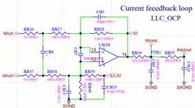
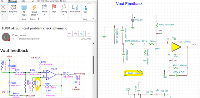
    Vout feedback

    Iout feedback


    Thank you.

    BR,

    Jenny

  • Hi Jenny, 

    When I click on the images they are very low resolution and I can't make out the component values. 

    Could you please clarify why you believe the device is entering thermal protection?

    You mentioned that this is a burn in test. While a temperature of 45 degrees C is within our recommended operating temperature range you also mentioned very high levels of current. Specifically:

    Input: 300 Vac / 50 Hz
    Output: 48 V / 90 A

    For this reason I would like to know the following:

    • What is the output current that is being demanded from the TLV9154
    • What is the input voltage to the TLV9154
    • What is the supply condition of the TLV9154
    • Any other relevant details would be appreciated. 

    This will help us understand if there is a power demand issue that is causing the die temperature to increase beyond the normal operating temperature. 

    If you can re-upload the schematic in a higher resolution that would also help us. 

    Best Regards, 

    Chris Featherstone

  • Hi Chris,

    Understood. Have send your schematic via mail.

    • What is the output current that is being demanded from the TLV9154 -> less than 1mA since only for signal (DC)
    • What is the input voltage to the TLV9154 -> Vcc=3.3V, th3 highest signal voltage is 3.3V as well
    • What is the supply condition of the TLV9154 -> LDO

    Please help to look into the issue. 

    Thanks a lot!

    Jenny

  • Hi Jenny, 

    The issue typically occurs after nearly 30 minutes of burn-in, at which point the IC temperature may rise above 90°C.
    From the waveform, it appears that a sudden rise in the OPA output may be causing the control malfunction. Since this phenomenon only occurs at high temperature, we suspect that the OPA may be entering thermal protection due to overheating.
    Ambient temperature: 45°C
    Input: 300 Vac / 50 Hz
    Output: 48 V / 90 A

    If the output current demand of the TLV9154 is less than 1mA and the supply is stable at 3.3V then I don't see how the die temperature is rising to 90 degrees C unless there is something unrelated to the OPA that is demanding a high amount of current on either its input or output. 

    Question:

    1. Is there anything in the circuit that is unexpectedly demanding high levels of current from the TLV9154?
    2. Is it possible that something in the circuit is causing an electrical overstress event onto the TLV9154?
    3. There are two circuits that were provided. Has the problem been isolated to one of the circuits? I suspect the Vout feedback circuit. See below. 
    We’d like to check if any recommend methods to reduce temperature? we want to try to control the thermal first time see if the issue can be resolved.

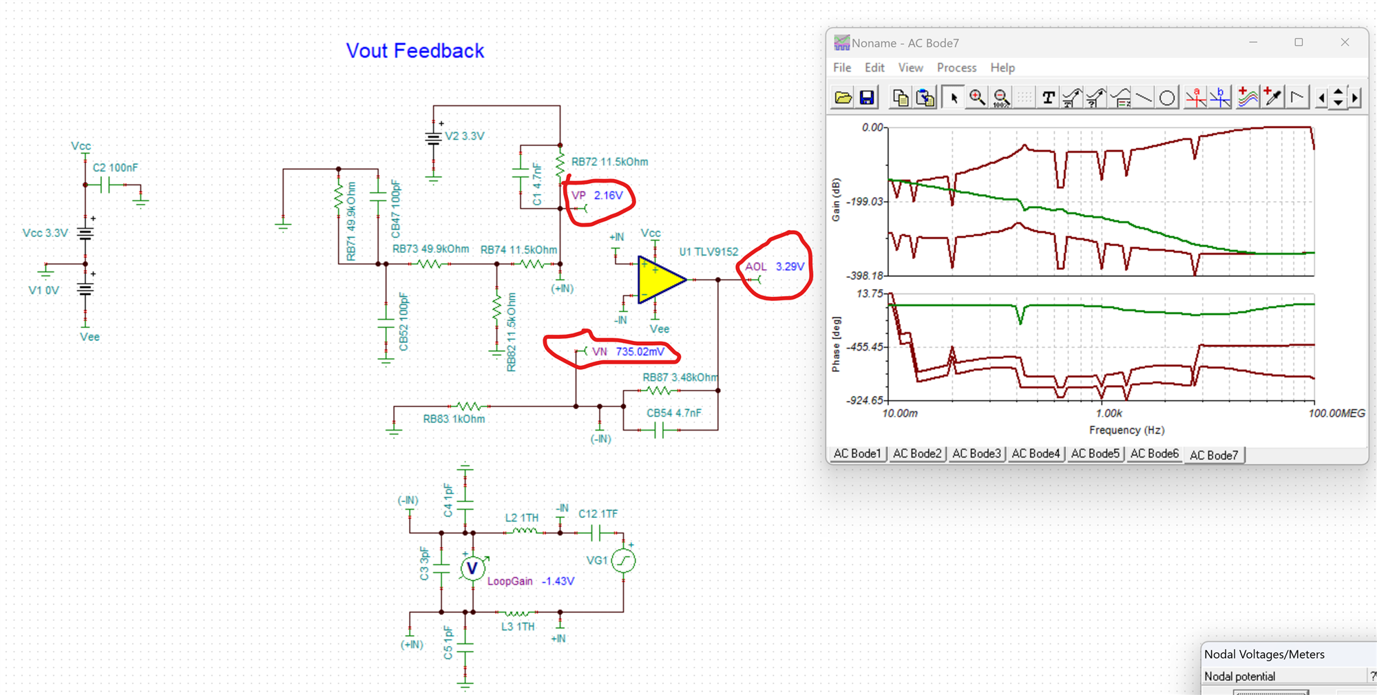
    I have simulated both circuits in Tina Ti. I see 3dB of gain peaking in the circuit. This potentially means that there could be a stability issue. It may be marginally stable at room temperature and then at hot it may go unstable. Or it is unstable and getting hot from being unstable. 

    Can the customer reduce the feedback capacitor CB54 to 3nF. Below I see a reduction in gain peaking with this value. See below. 

    TIna Simulations

    TLV9154 Vout Feedback.TSC

    TLV9154 Iout Feedback.TSC

    Best Regards, 

    Chris Featherstone

  • Hi Chris,

    Thanks a lot for your detailed reply.

    1. Is there anything in the circuit that is unexpectedly demanding high levels of current from the TLV9154? In theory, this should not be the case, since this circuit design is reused from other products and should not introduce any additional high current demand.
    2. Is it possible that something in the circuit is causing an electrical overstress event onto the TLV9154? The TLV9154 is used for small-signal processing, so there should not be any overload condition.

    The OAP input is connected to Vout, and under the current condition, Vout is stable at 48V.


    The customer followed the recommendation to reduce CB54 to 2.2nF. However, the test results became worse. After approximately 30 minutes of burn-in, the OPA output still increases abnormally, falsely triggering protection and causing a restart.

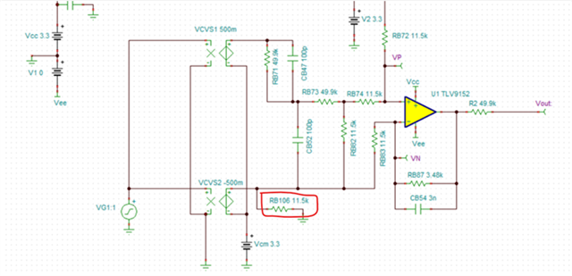
    It was also found during circuit simulation that one component had an incorrect resistor value. The circled resistor is actually 0 ohm.


    May I have your help to re-run the simulation to check if there are any possible adjustments to improve circuit stability. I'm asking the customer to temporarily remove or isolate nearby heat-generating components to evaluate whether elevated IC temperature is contributing to the issue.

    Thank you.

    Best Regards, 

    Jenny

  • Hi Jenny, 

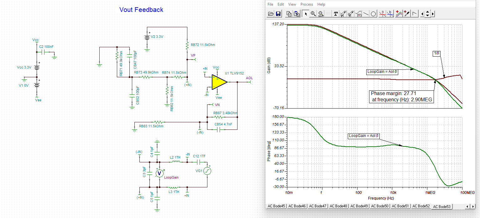
    I have done a thorough stability analysis. What I found is that the input resistors are very high and interacting with the beta network and the input capacitance such that a zero occurs in 1/beta. This causes the phase margin to be 27.71 degrees which is unstable. Because this is an interaction with the beta network and the input capacitance, changing the feedback capacitor has little affect. 

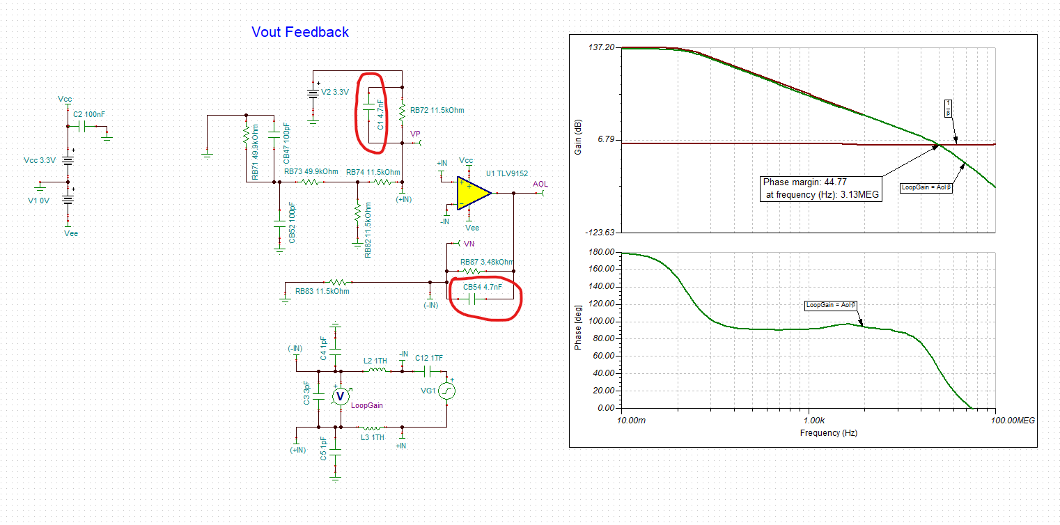
    I found that you have two options

    1. Reduce all the resistors by a factor of 10
    2. Or add a capacitor across RB72 that is the same value as the feedback capacitor. 

    My second simulation below shows option 2. Notice that my phase margin is now 44.77degrees which is an improvement from the original circuit that has 27.71 degrees. For this reason I believe there is a stability issue that is contributing to the problem. I have attached my Tina simulation below as well. 

    Unstable:

    Stable

    Tina Simulation

    Open Loop Stability-TLV9152.TSC

    Best Regards,

    Chris Featherstone

  • Hi Chris,

    Thanks for your explain,


    Is the result for OPEN Loop of OPA, which are effected by input resistance and capacitor design ?

    What phonemes is effect caused by phase margin 27.71deg at higher frequency 2.9MHz? will see a oscillation with higher frequency on output waveform?

    Just check RB83 is 1K. May I have your help to clarify the stability again for Vout feedback again?

    Can you also to simulate the output current circuit? shown as below, Thanks a lot!!

    Best Regards,

    Jenny Chen

  • Hi Jenny, 

    Is the result for OPEN Loop of OPA, which are effected by input resistance and capacitor design ?

    The method shown for breaking the loop is outlined on page 27 in https://www.ti.com/jp/lit/wp/sboa626/sboa626.pdf. This application note covers every aspect of op amp stability, The purpose of using this method in simulation is to isolate the open loop gain AOL, the feeback network beta and 1/beta, and the loop gain Aol*beta. Isolating these parameters helps us determine where poles and zeros are occurring in the entire circuit. In this case I observed that there is a zero in 1/beta that was causing the circuit to be unstable. 

    What phonemes is effect caused by phase margin 27.71deg at higher frequency 2.9MHz? will see a oscillation with higher frequency on output waveform?

    A phase margin of less than 45 degrees is typically considered indicative of an unstable circuit. When a circuit is unstable, its behavior becomes unpredictable and it will not respond as expected. In other words, the circuit's performance will be compromised, and it may exhibit oscillations, ringing, or other undesirable effects.

    Note that a phase margin is a measure of the amount of phase shift between the input and output signals of an amplifier, and it's an important indicator of stability in feedback circuits. A phase margin of 45 degrees or more is generally considered sufficient to ensure stability, while a phase margin of less than 45 degrees can lead to instability and unpredictable behavior.

    Just check RB83 is 1K. May I have your help to clarify the stability again for Vout feedback again?

    When I change to the 1k resistor I see that the circuit no longer functions. The inputs are ripped apart which means the op amp rails out on its output. The frequency response no longer applies because the op amp is not in it's linear operating range. See below. 

    If I understand the goal of this circuit we may be able to provide some guidance on how to change the design to get it operating in its linear operating range.

    1. What is the expected gain of this circuit? 
    2. What is the expected input signal to this circuit?
    3. What is the purpose of the RC network on the input with the 49k ohm resistors etc?

    Before I investigate the Iout circuit I would like to resolve this circuit first before we look at too many details at once. 

    Best Regards, 

    Chris Featherstone

  • Hi Chris,

    Checked the customer, they're used 1K for RB83.

    1. What is the expected gain of this circuit?  --> They're designing -60~-40Vin to 0~3.3Vout
    2. What is the expected input signal to this circuit? --> -60~-40Vin
    3. What is the purpose of the RC network on the input with the 49k ohm resistors etc? To ratio the -60~-40V transfer into 0~3.3V.

    Customer need us to support to design the parameters to enter the stable range. Please help.

    One thing want to check. Do you have waveforms which demo Vout when occurs Thermal Protection? The customer also want to check if this thermal problem. Since their Vout went high, but datasheet shows output is High-Z.

    Thanks a lot!

    Jenny

  • Hi Jenny, 

    We don't have waveforms to demonstrate the thermal protection. The Iq will drop when the device enters thermal shutdown however. If they have the ability to measure Iq on the part in system then it will decrease during thermal shutdown events. 

    I have successfully simulated and verified the circuit parameters using the TLV9152 on a single 3.3V supply. 

    1. What is the expected gain of this circuit?
    • System Gain: -16.1 dB (Linear Gain: 0.156 V/V).
    • Performance: This gain effectively scales the 20V input swing down to a 3.12V output swing. This provides a small amount of "headroom" below the 3.3V rail to ensure the op amp remains in its linear region and avoids signal clipping.
    1. What is the expected input signal to this circuit?
    • Input Range: -60V to -40V DC.
    • Resulting Output:
      • At -60V Input: ~0.01V Output
      • At -40V Input: ~3.12V Output

    Level Shifting: Since the TLV9152 operates on a single 3.3V supply, it cannot process negative voltages directly. The resistor network (specifically the 182k ohm input and 10k ohm reference resistors) acts as a summing attenuator. It "lifts" the negative -60V/-40V signal into a safe, positive range (0V to 1.04V) before it reaches the op amp.

    Filtering: The 4.7nF capacitor in the feedback loop creates a low-pass filter with a cutoff frequency of approximately 1.7 kHz. This ensures a stable output by removing high-frequency noise and preventing oscillation.

    Design Parameters for the Stable Range
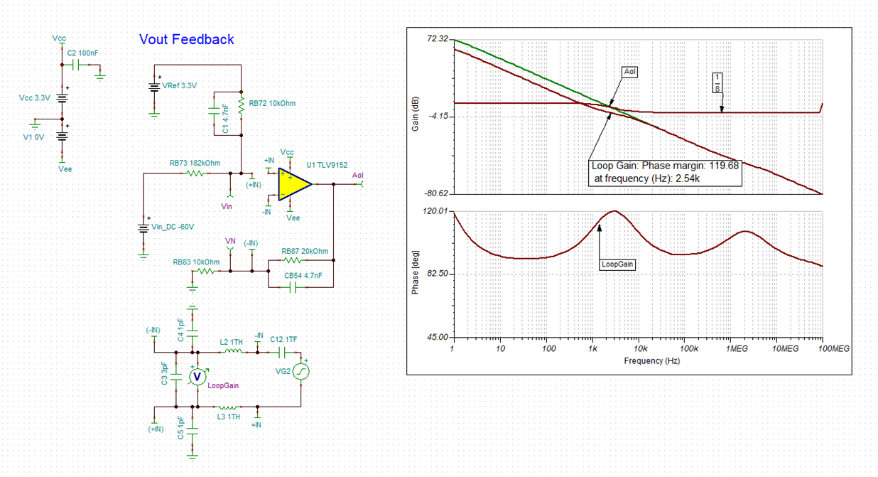
    To ensure the op amp stays in the stable, linear operating range (without saturating against the power rails), the component values were utilized in the simulation below. I have swept -60 to -40 on the x-axis of the first image while measuring the output of the op amp. This achieves the desired design goals. In addition I do not see gain peaking like we did before in the Gain vs Frequency curve. 

    I have matched the reference resistor and the gain set resistor below to be 10k each. Matching Rg and Rref at 10kΩ ensures the op amp is perfectly balanced, which maximizes the Common-Mode Rejection Ratio (CMRR) to filter out environmental noise and ensures Ib on R doesn't pull the inputs apart. 

    I have also checked the stability and the phase margin is very good at 119.7 degrees. 

    Included below are my Tina simulations for this updated design. 

    TLV9152 Vout CKT.TSCStability TLV9152 Vout CKT.TSC

    Best Regards, 

    Chris Featherstone