Part Number: INA700
Hi all,
The INA700 datasheet states:
"When connecting the A0 pin to SDA to set the device address, an additional hold time of 100ns is needed on the MSB of the I2C address to provide the correct device addressing"
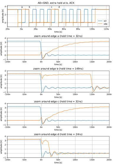
In our testing, this hold time needs to be added between the first falling edge of SCL, and SDA rising for the MSB of the address.
In the diagram below, we have added hold time at point 'a' whereas the datasheet appears to mean it should be added at point 'b'.

Adding holdtime at point 'b' is not possible with our I2C controller (and likely most hardware based I2C controllers) because once the controller and data is configured, it will run at the specific clock rate with no opportunity to add hold time to bits.
Is what we are doing valid? Is it correct and guaranteed to work reliably?
Thanks,
Richard.