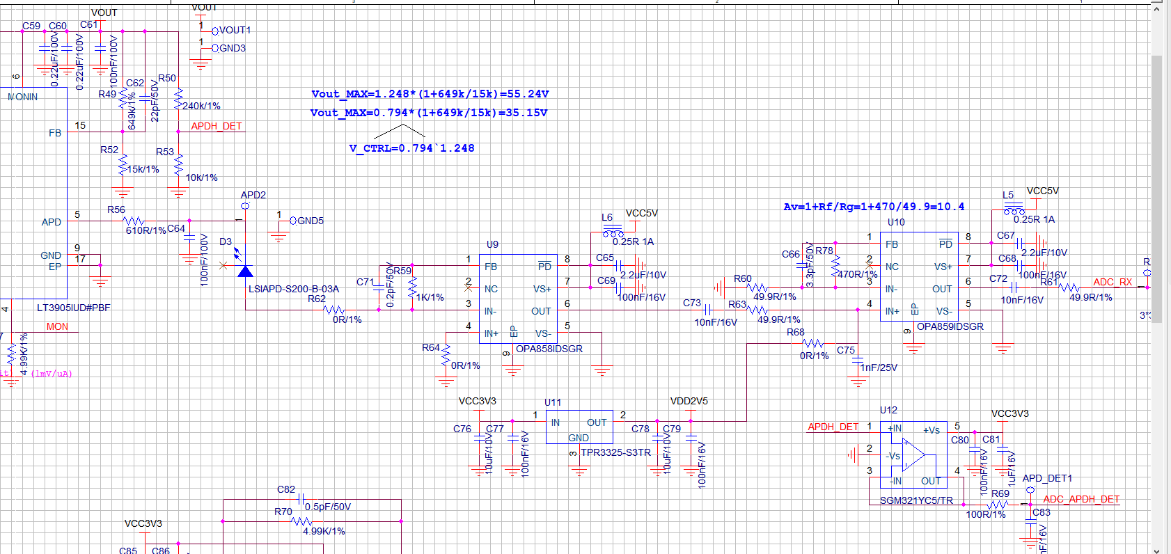
This thread has been locked.

If you have a related question, please click the "Ask a related question" button in the top right corner. The newly created question will be automatically linked to this question.

OPA858: Application issue.

Expert 2230 points

Part Number: OPA858
Other Parts Discussed in Thread: THS4541, OPA859

Hi Team,

1. Should the Vref of OPA858IDSGR be connected to a 2.5V bias voltage or to ground? If OPA858 is used as a transimpedance amplifier (TIA), is the output voltage formula: Vout_TIA = Vref - Iapd × Rf?
2. Is the Vref of OPA859IDSGR connected to a 2.5V bias? The signal input range of the ADC on the main control board is: differential signal: ±0.5V (1Vpp differential).
3. This is the receiving circuit of the LiDAR. Could you please help check if there are any issues with the schematic design?

OPA858.jpg

  • Hello Reed,

    1. Yes, that is correct. Vref should be connected to 2.5V bias voltage to properly bias the TIA to mid-supply. How large of a DC current are you expecting from your PD? If you are expecting a wide range, I would suggest having a DC bias voltage you can adjust at the IN+ of the amplifier and can be controlled either digitally or analog. The bias at the input will satisfy your input common-mode voltage range of your amplifier. While, the PD DC and VREF at IN+ will need to satisfy your output voltage range of the device. 

    2. Yes, in the schematic the OPA859 is correctly connected to a 2.5V reference. If you are following a differential ADC after the OPA859, I would recommend driving the ADC with a fully differential amplifier such as the THS4541. Our fully differential amplifiers make it easy to correctly bias the voltage at the output via the VOCM pin to the ADC. You would route the ADC reference pin to VOCM which will then correctly set the DC voltages for the FDA and ADC. Then full scale voltage can be set via the gain/attenuation at the FDA stage. Here is a quick app note on the configuration: https://www.ti.com/lit/an/slyt773/slyt773.pdf?

    3. I do not see any concerns with the schematic except what you already pointed out for the answer in 1) for your input and output common mode voltage specification. Here is a resource on LiDAR applications using the OPA85x family that might be useful for any other parts of your system: https://www.ti.com/lit/ab/sboa337a/sboa337a.pdf?

    Thank you,
    Sima