This thread has been locked.

If you have a related question, please click the "Ask a related question" button in the top right corner. The newly created question will be automatically linked to this question.

TLV3607: Subject: Propagation Delay Mismatch Between Datasheet and Board Measurement – Request Test Conditions

Part Number: TLV3607

Hi TI team , 

We would like to bring to your attention a concern regarding propagation delay observed in our hardware compared to the values mentioned in the datasheets.

We selected the below components in our design based on the propagation delay specifications provided:
• Comparator: TLV3607RTER
Datasheet propagation delay: ~800 ps
• LVDS to TTL Converter: SN65EPT21DGKR
Datasheet propagation delay: ~1.44 ns

However, in our actual board measurements, we are observing:
• Comparator propagation delay: ~4.5 ns
• LVDS to TTL propagation delay: ~3 ns

Due to this increased delay, our system-level timing requirement is not being met.

We request your support in providing the exact test conditions under which the datasheet propagation delay values are achieved, including:
• Supply voltage conditions
• Input signal amplitude and edge rate (rise/fall time)
• Output load conditions
• Temperature conditions
• Measurement method and threshold levels

Additionally, we would appreciate your guidance on how to configure our test setup or board conditions to achieve propagation delay closer to the datasheet values.

This information will help us correlate our measurements and determine if any design or measurement setup changes are required from our side.Subject: Propagation Delay Mismatch Between Datasheet and Board Measurement – Request Test Conditions
 

  • Hi Mohankumar,

    Could you please share your schematic and waveforms for your propagation delay measurements? Could you also please include how you're making your measurements?

  • HI team, 
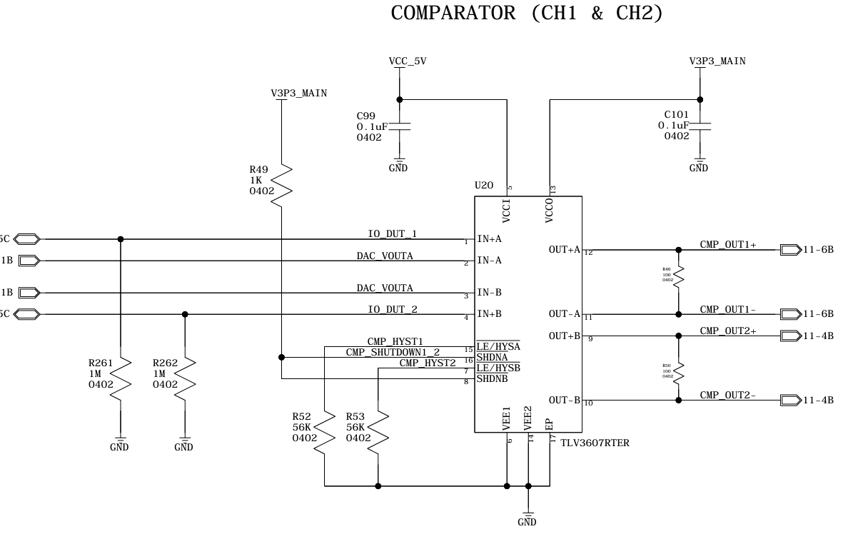
    I have attached the schematic and waveform for the comparator and LVDS to TTL converter below.


  • Hi Team, 

    I have attached the schematic and waveform for the comparator and LVDS to TTL below, 


    attached waveform is for total Pd of comparator input and lvds to ttl output.
    first probe is comparator input and second probe is LVDS to TTL out put so we get the PD total is above >5.5ns.

  • Hi Mohan,

    Thank you for sharing the schematic and the oscilloscope waveforms.

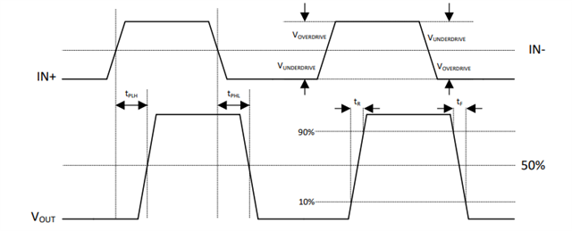
    Could you please tell me what DAC_VOUTA is driven to so that we can tell what the switching threshold is for the TLV3607? This is important as propagation delay is dependent on the overdrive and underdrive of the input signal. In general, comparator propagation delay increases (slower) with more underdrive and decreases (faster) with more overdrive.

    I'll make some comments about a few things I noticed below:

    1. It looks like there is a 56kΩ resistor connected to both the nLE/HYSA and nLE/HYSB pins of the TLV3607. This introduces ~60mV of internal hysteresis to each channel of the comparator. This means that the high to low and low to high switching thresholds are DAC_VOUTA - 30mV and DAC_VOUTB + 30mV respectively.

    Implementing hysteresis effectively increases the underdrive of your input signal since the switching threshold "moves away" from the IN+ voltage based on the output state.

    If the hysteresis is not necessary in your application, I'd recommend reducing the internal hysteresis of the comparator by depopulating R52 and R53:

    There is also another thing about the way propagation delay is being measured by the oscilloscope. Unless properly configured, the delay measurement on the oscilloscope usually measures mid-point to mid-point delay of your two channels, but the actual crossing point of IN+ and IN- of the comparator starts at DAC_VOUTA - 30mV and DAC_VOUTB + 30mV (due to the hysteresis) depending on low to high or high to low propagation delay. To get an accurate measurement of the propagation delay, you need to make sure that the starting point for your delay measurements happen at the hysteresis thresholds instead of mid-point to mid-point.

    2. Overall propagation delay seems high, but I'd like to distinguish the delay contributions of each device (comparator and translator). Could you please probe IO_DUT_1 (IN+), VOUT_DAC1 (IN-), CMP_OUT1+ (OUT+A), and CMP_OUT1- (OUT-A), and measure the delay from the from input to output of the comparator? Please zoom in on a single period, and make sure all signals are referenced to GND as I'd also like to see the output common mode of the comparator to ensure that we are providing the correct signal levels to the translator.

  • Hi team,


    Our Conditions:

    IO_DUT_1 IN+A will be in 0.8V to 5V 
    DAC_VOUTA IN-A will be in 0V to 5V

    Please share details, at what condition we can expect the PD 800ps mentioned in datasheet.


  • Hi Mohankumar,

    I am a little confused, are both comparator inputs swinging at the same time? Again, signal swing is very important in the propagation delay of both devices.

    Measurements are typical at data sheet test conditions:

    VCCI = VCCO = 2.5 to 5V, VEE = 0V, VCM = VEE + 300mV, RLOAD = 100Ω, CL = 1pF probe capacitance, typical at TA = 25°C (unless otherwise noted). Propagation delay measured at 50mV overdrive and underdrive with a 50MHz square wave.