This thread has been locked.

If you have a related question, please click the "Ask a related question" button in the top right corner. The newly created question will be automatically linked to this question.

OPA333: Opamp selection

Part Number: OPA333
Other Parts Discussed in Thread: OPA350, OPA330, OPA320


Hi,


I am using OPA333 to drive the Microcontroller ADC. Do I need to connect an RC filter at the output of the OPAMP. Or can I connect directly to uC ADC.

Most probbly I will change this opamp to OPA350, but my question remains the same.


image.png


  • You do not need RC filter but typically one uses RC filter to optimized circuit performance based on the details of ADC input, required bandwidth, resolution and sampling frequency - please see the training material under following link: 

    https://www.ti.com/video/series/precision-labs/ti-precision-labs-analog-to-digital-converters-adcs.html?keyMatch=driving%20ADC&tisearch=universal_search

    There is a world of difference between a zero-drift OPA333 (chopper amplifier with GBW of 350kHz) and much faster OPA350 with GBW of 38MHz.

    If you are not concerned about the sampling rate, signal frequency, resolution, etc. a good rule of thumb is to add 1nF cap in front of ADC.  

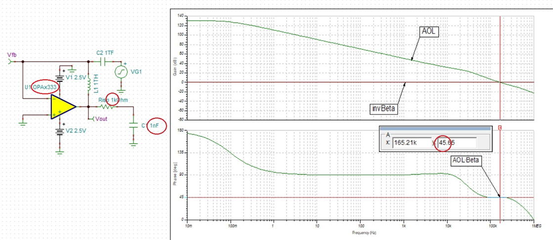
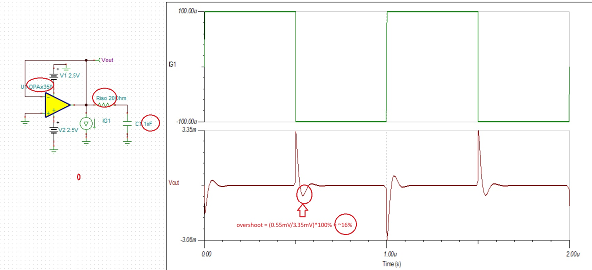
    However, in order to drive 1nF load, OPA333 would require 1kohm Riso while OPA350 would need only 20 ohm - see below.

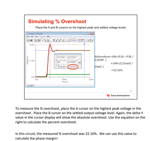
    BTW, it is recommended to assure a minimum 45 degrees phase margin and/or less than 25% small-signal overshoot - see Stability training material under following link:

    https://www.ti.com/video/series/precision-labs/ti-precision-labs-op-amps.html

    OPA333 AC Stability Buffer.TSC

    OPA333 Transient Stability Buffer.TSC

    OPA350 AC Stability Buffer (1).TSC

    OPA350 Transient Stability Buffer.TSC

  • Hi Marek,

    Below is the reason why I am changing OPA333.

    " In my circuit, I am using an OPA333 op‑amp to buffer a sensor signal before it goes through a two‑stage RC low‑pass filter (R13–C44 and R14–C45). My simulation shows the overall filter bandwidth is around 45 kHz.

    The microcontroller I’m using is a Microchip SAM‑D5x/E5x device, which has a 12‑bit, 1‑MSPS SAR ADC. Since this type of ADC uses an internal sampling capacitor, the op‑amp must have enough bandwidth, slew rate, and output drive to charge that capacitor quickly and settle before each conversion.

    The OPA333 datasheet states that it has:

    • Gain‑bandwidth = 350 kHz

    • Slew rate = 0.16 V/µs

    • Output drive ≈ 5 mA

    But for a 45 kHz, 3.3 V full‑scale sine wave, the required slew rate is:

    SR_required = 2π × 45 kHz × 1.65 V ≈ 0.455 V/µs.

    This required slew rate (0.455 V/µs) is almost 3× higher than what the OPA333 can provide (0.16 V/µs)."

  • Please see my comments:

    The suggested RC has a small-signal cut-off frequency pf 159kHz. Thus, more than enough to accommodate filter bandwidth of 45kHz - see below. However, you are correct that OPA330 full-power bandwidth (slew rate) is too low to avoid slew induced distortion. 

    Even more importantly, in order to settle the signal to 12-bit resolution within sampling rate of 1MHz would require op amp with much higher GBW like OPA350 or OPA320. This is the reason why you should review following training material:  https://www.ti.com/video/series/precision-labs/ti-precision-labs-analog-to-digital-converters-adcs.html?keyMatch=driving%20ADC&tisearch=universal_search

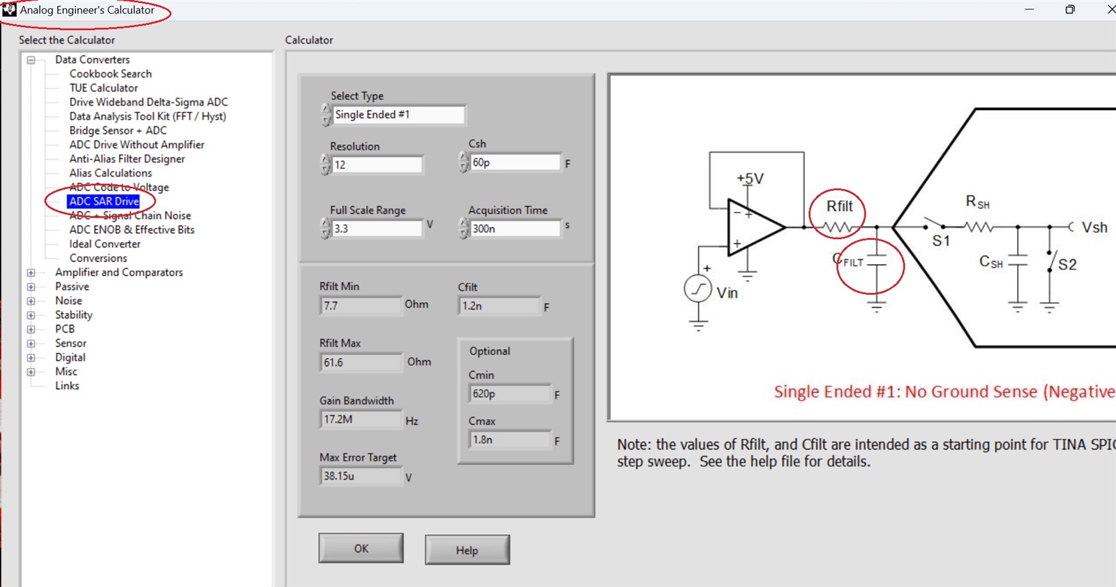
    Additionally, please download Analog Engineer's Calculator so you may use it to optimized the RC filter for required sampling rate and resolution:

    https://www.ti.com/tool/ANALOG-ENGINEER-CALC

  • Hi Marek,

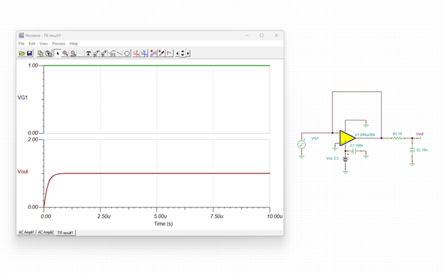
    I am palnning to use OPA350 as shown below.

    opa350-1.TSC

    STEPRESPONSE:

    No ringing. I believe it is stable.

    Regards

    HARI

  • Hari,
    OPA350 shows 69 degrees phase margin with Riso of 10ohm driving 15nF cap, thus is pretty stable.
    A small-signal transient analysis confirm solid stability (make sure you look at correct Vout location - see below).
    However, a sampling rate and effective small-signal bandwidth are completely different concepts.  In order to achieve 12-bit resolution at 1MHz sampling rate the system must be able to settle to 1/2 LSB of 12-bit resolution of  1/(2^13) = 0.000122
    Since output,   , the settling time is a function of RC time-constant,Ƭ=R*C, and in your case Ƭ=10*15e-9 = 150ns

    Therefore, settling to 12-bit resolution means:  

    e^(-t/Ƭ) = 0.000122

    -t/Ƭ = ln( 0.000122)

    t = -ln (0.000122)* Ƭ = 9.01* Ƭ

    Thus, it takes 9 time constants to settle to 12-bit resolution. This means that the minimum acquisition time would need to be: t = 9.01* = 9.01*(10*15e-9) =1.35us
    Clearly, with 10ohm and 15nF the required setting time to 12-bit resolution is 1.35us; thus, it would not be possible to run it at 1MHz sample rate. For this reason you need to use ADC SAR drive optimization tool (see above) to help you determine what R and C you need to use to meet your system requirements.

  • Hi Marek,

    I used Analog engg calc. My result is given below.

    A small-signal transient analysis confirm solid stability (make sure you look at correct Vout location - see below).

    May Iknow how you are predicting stability using this method. 

    Is it percentage overshoot vs phase margin.

    Regards

    HARI

  • I previously included link to our Circuit Stability training material - here it is again:

    www.ti.com/.../ti-precision-labs-analog-to-digital-converters-adcs.html

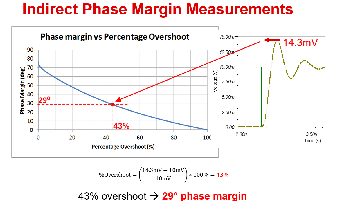
    The relation between the small-signal overshoot and phase margin comes from approximation of 2nd-order graph shown below.  In order to assure stable operation over temperature and process variation, the recommendation is to design for a minimum 45 deg phase margin or maximum 25% small-signal overshoot.

  • Hi Marek,

    Thank you for your support.

    In the training videos for transient analysis a step voltage is applied at the opamp input.

    In your circuit a current step is applied at the output of the opamp.

    May I know can I use this method for all opamp circuits or only specific to opamps which is driving a capacitive load.

    Regards

    HARI

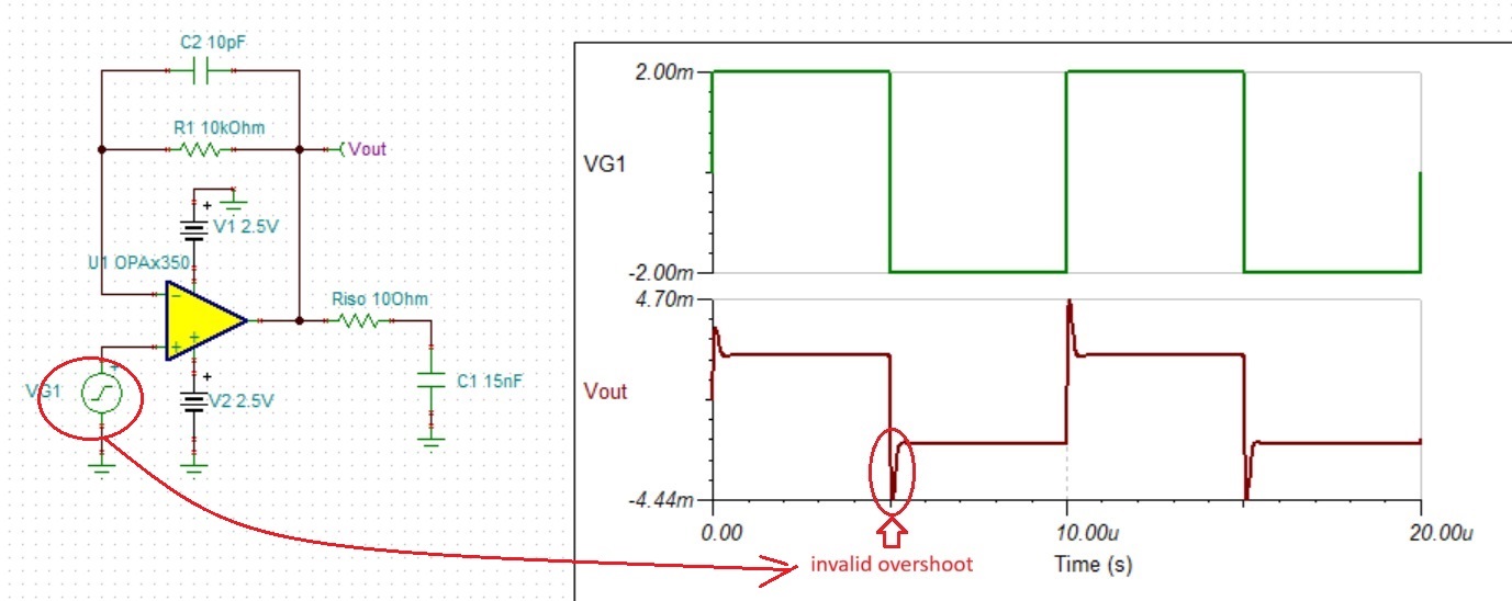
  • For as long as there is no passive components in the signal path (to filter out the input signal), as is the case here, the output gets disturbed with a step signal in either case.  Thus, it does not matter whether you excite the output with the input voltage step or output current pulse - they both should give you the same percent overshoot. 

    However, if there is any RC filter between input and output you must excite the output directly with the square current pulse to give you a valid overshoot number - see below.

    For this reason it is preferable to excite the output, which always give you a correct percent overshoot.

  • Hi Marek,

    What I understood is the following:

    For a general op-amp transient analysis, applying a step voltage at the input is the standard method because it evaluates the closed-loop response of the amplifier, including overshoot, ringing, and settling.

    However, when the op-amp is used to drive a capacitive load or a SAR ADC input, the dominant disturbance often comes from the output side, not from the input side. In that case, the ADC sampling action is better represented by a current/charge pulse at the output node.

    So, for this type of circuit, applying a current step at the output is more representative because it directly tests the op-amp + load interaction and shows whether the output remains stable when the load suddenly draws current.

    My understanding is also that if there are no passive components in the signal path between the op-amp output and the load, then an input-step test and an output current-step test may give similar overshoot behavior. But if there is a series resistor, RC network, or capacitor between the op-amp output and the ADC/load node, then an input-step response may not accurately represent the real load-transient stability. In that case, exciting the output directly gives a more valid overshoot result.

    So the conclusion I understood is:

    • Input voltage step is appropriate for general amplifier transient analysis.

    • Output current step is more appropriate when checking ADC-driving or capacitive-load stability.

    • This method is not meant for all op-amp circuits, but is especially useful when the main disturbance comes from the output/load side.

    Please let me know if this understanding is correct.

    Regards

    HARI

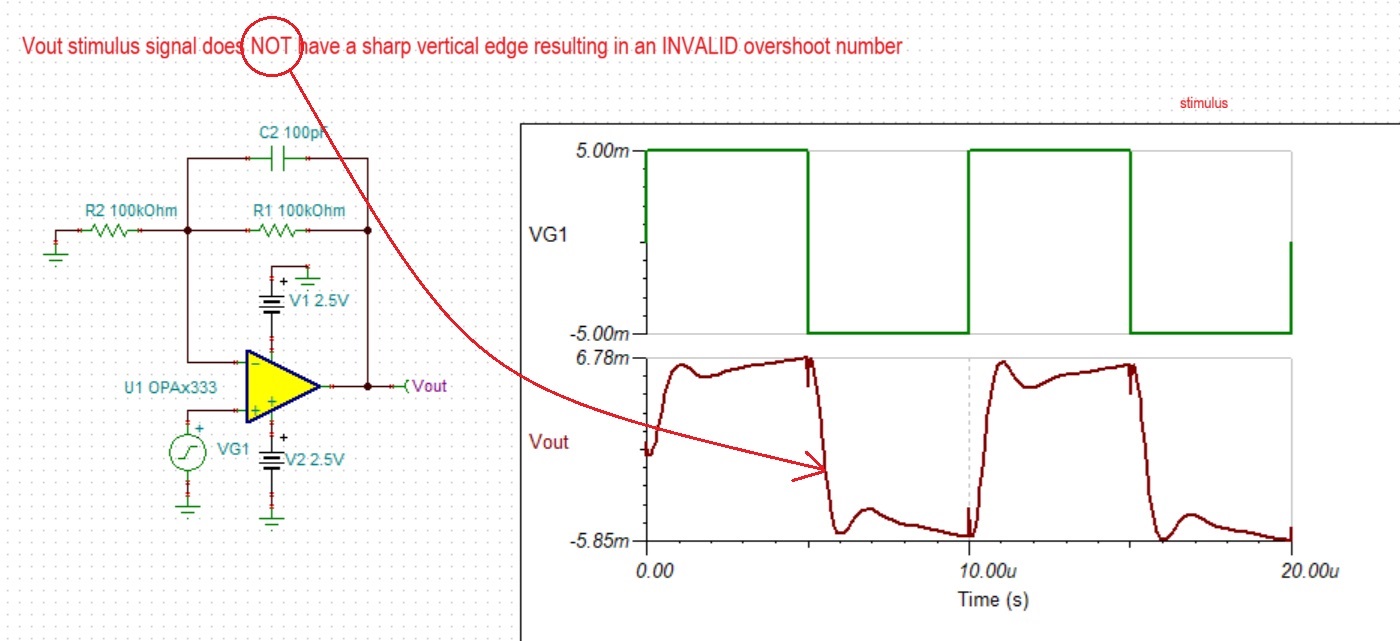
  • The issue is simpler than what you describe. In order to determine stability by means of small-signal overshoot, its output must be stimulated by step (sharp edge) signal; thus, any RC between inverting input and output resulting in rounding-off the edges makes the measurement invalid - see below.

    For this reason it is best to always directly stimulate the output with current pulses in order to avoid rounding-off edges of excitation signal.

  • Hi Marek,

    Please don't feel bad. I will ask my question in another way.

    For a simple inverting amplifier with a capacitor across the feedback resistor and no capacitive load at the output, what is the correct way to check stability? Should I use an input step or an output current pulse?

    Regards

    HARI

  • It's always correct to use current pulse at the output for determining overshoot number because it directly forces Vout to have sharp edges. If feedback RC is low, it may make no difference and either method could work.  But if the feedback RC between the inverting input and output is relatively large (e.g.100k||100pF) that results in slowing the edges of stimulus Vout signal, it makes the overshoot measurement for stability purposes invalid  - see below.

    On the other hand applying the stimulus directly to Vout result in a valid overshoot number - see below.

  • Hi Marek,

    Thank you very much. That is clear for me.

    May I know how toslect the current pulse amplitude and frequency.

    I believe the frequency is based on the ADC sampling rate (in thisapplication ), please correct me if I am wrong.

    How about the amplitude? why 2uV Peak to peak , why not 2mV or 2V.

    Regards

    HARI

  • The current pulse magnitude depends on the op amp output impedance and thus must be adjusted to result in few mV output step stimulus signal (<+/-10mV) so the op amp operates in its linear region and does  NOT slew.

    The frequency of the current pulse signal depends on the capacitive load and thus needs to be adjusted so you can clearly see the initial stimulus signal magnitude (first peak) followed by the system response second peak output signal magnitude: then overshoot = (second_peak/first_peak)*100%.