This thread has been locked.

If you have a related question, please click the "Ask a related question" button in the top right corner. The newly created question will be automatically linked to this question.

INA241A: INA240A1 Reference inputs 1v65

Guru 56358 points

Part Number: INA240A
Other Parts Discussed in Thread: TPS717

Hello team,

We noticed when the two REF input pins are tied together and the IC is placed on PCB with 3v3 applied the REF inputs are floating 1v65 with no connections to an external reference. 

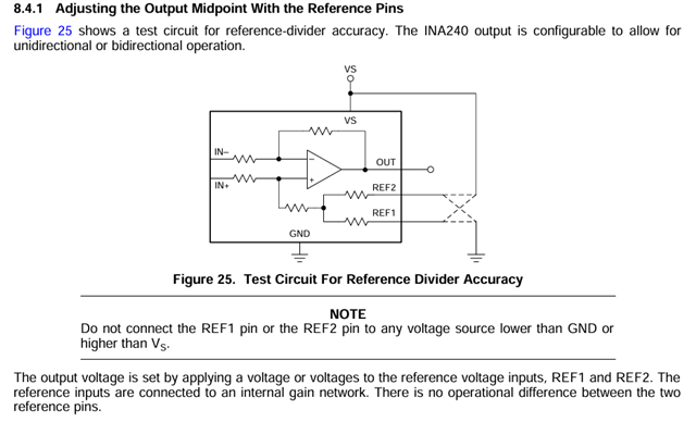
Seemingly the internal REF circuit does not require any external voltage when the two REF1/2 pins have been tied together. This observation contradicts the datasheet notes on how the REF inputs need an external bias voltage.

  Are we actually adding noise into the amplifier by connecting an noisy 20KHz extern DAC to the REF1/2 inputs when they are already at 1v65 bias level? Do we actually need to force 1v65 bias on REF1/2 pins when they are on same PCB with 3 amplifiers REF1/2 inputs tied together via copper traces? Can we just leave the REF1/2 tied pins floating at 1v65 or will the bias follow the input/s signal? 

Thanks in advance for investigating this very strange observation! 

  • Hi Genatco,

    The VREF pins will sit around Vs/2. However, this is not accurate nor is it able to drive anything. These are high impedance pins. 

    It is recommended that you drive the Vref pins with the voltage you want. It should not be trusted that the Vref pins will stay at the nominal value of 1v65.

    Best,

    Holly

  • Hi Holly,

    That makes sense but was a bit alarming to see the 1v65 floating on the REF pins. 

    These are high impedance pins. 

    Yet as you stated, REF1/2 input pins are bias into the amplifier first stage transistors BJT's? The REF pins exposed to the outside seemingly for Unidirectional control of the output. So very tiny current is required to bias the REF input of the amplifier? Why are they already biased +1v65 if bidirectional output current is being measured? Are we just adding a noise source to REF1/2 pins that is causing the amplifier to behave badly?

    Holly, Can you test this hypothesis in TI laboratory and verify why REF1/2 need to be connected +1v65 DC supply when Bidirectional output mode is the default behavior of the input stage? It simply does not make sense REF1/2 pins and Noninverting input is floating at a pre biased level +1v65. Most all bidirectional current monitors do not require outside precision +1v65 reference voltage source. Note our PCB has Noninverting input shunts very near ground level albeit 10Ω resistors exist before ±IN pins.

    What in the internal amplifier is setting the REF1/2 pins +1v65 without any external current source? Why should we add another noise source into the amplifier? Have you examined the internal circuit diagram to explain why there is already bias when REF1/2 pins are tied together?

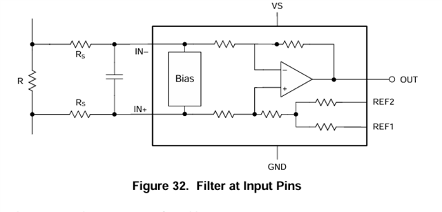
    This concern as the transient response is far too sensitive for low side shunt current monitoring even with 10Ω 1nF filter at ± inputs and 10nF bypass on VS pins. We notice output spikes that exceed supply and the DC inverter stage is very dampened, no overshoot, <-4v undershoot on the MOSFET turn on events. The +3v3 VS pins are being supplied by dedicated LDO TPS717 Ultra-High PSRR:– 70dBat1kHz, 67 dB at 100 kHz, and 45 dB at 1 MHz 

    Why is the INA output transient response ringing 20-26MHz with 16-20KHz PWM signal crossing the shunts? If they truly reject PWM then the output should not be so responsive to PWM signals let alone ringing 20-26Mhz! 

  • Hi Genatco,

    You are correct, only a small current is needed to bias the REF pins. The block diagram shown in the datasheet is simplified. In reality we have a fully differential input stage which causes the voltage on the REF pins to sit about mid-supply. For most instances the REF pin voltage should stay at mid-supply, but leaving the REF pins floating is the same as leaving the input of an amplifier floating which is not a good practice. If anything couples into the REF pins you are going to throw off your output voltage.

    This device is designed to reject common-mode PWM, not differential. However, the 20kHz is slow enough that we should be able to track it fine. Can you please share a schematic of this? I would suspect the ringing you are seeing is coming from too much capacitance on the output.

    Best,

    Holly

  • REF pins floating is the same as leaving the input of an amplifier floating

    Yet they are coupled through a resistor on non-inverting input and to the shunt at ground level. The concern is connecting noisy reference signal to the REF1/2 pins tied together other than 1nF capacitor to ground is going to inject noise into that input. In the past tied the REF2 to VS pin REF1 through 0R to ground and somehow that seemed to invert the output. And tied together inverts the output when +IN connects to ground via the shunt. 

    fully differential input stage which causes the voltage on the REF pins to sit about mid-supply.

    Yet the pins are exactly +1.67v and I have to wonder exactly how that is occurring if it was not a design mistake to have current flowing back out the REF pins when the Default mode of operation appears to be Bidirectional output signal. Connecting REF1 to ground near the shunt +IN seems to me a bad design practice! There are the same high frequency transients seen DC inverter switching BEMF, anything we can do to quiet the INA output is a wining scenario. It's unclear where the HF is getting into the system as there are snubbers on each of the NFETS and soft PWM commutation via the gate drives.  

    I would suspect the ringing you are seeing is coming from too much capacitance on the output.

    Best,

    Only 1nF ceramic near INA output and 100pF ceramic tied to ground at the launch pad header through typical 0R. The faulting transients are inside the HF when the NFETS are turning on and off. The input filter looks the same as the datasheet diagram.   

  • Dear Holly,

    but leaving the REF pins floating is the same as leaving the input of an amplifier floating

      Actually, I discovered DACA +1v65 from launch pad MCU was not really producing +1v65. The peripheral clock was not enabled and DACA output was floating when I disconnected the INA's REF pins. The +1v65 originated from REF1/2 pins being tied together. Even put 10nF capacitor at DACA header pin to ground and calmed the noise coming from all the REF pins, even with the motor running they remained +1v65. Seemingly the REF pins jumper wire to the DAC on the launch pad was acting like an antenna? 

      Have to admit this really fooled me and was not expecting REF1/2 pins to be outputting +1v65 as the datasheet makes no mention. I'm very upset because whatever laboratory personnel detailed the function of the REF pins missed this detail or simply didn't care to mention it to TI engineers. Perhaps it's time to add this detail into the datasheet reference pins section. 

  • Hi Genatco,

    Thank you for all of this insight. I will pass this along to our systems team so we can get this resolved in the future.

    Best,

    Holly